Contents
PCB assembly quality cannot usually be verified with a single method. Visual inspection and automated optical inspection (AOI) detect visible workmanship and placement defects, X-ray inspection evaluates hidden solder joints, in-circuit testing (ICT) checks electrical nodes and selected component characteristics where test access exists, and functional testing verifies whether the assembled board performs its defined functions. An effective PCBA test plan combines methods according to package visibility, expected defect modes, electrical access, product risk, production volume, and customer acceptance requirements.
PCB Assembly Testing Methods at a Glance
| Method | Primary purpose | Typical defects or issues detected | Best fit | Main limitation |
|---|---|---|---|---|
| Visual inspection | Check visible workmanship and mechanical assembly | Missing or damaged parts, polarity errors, visible bridges, connector and hardware issues | First articles, manual operations, final workmanship review | Coverage depends on line of sight and inspector consistency |
| AOI | Compare visible assembly features using cameras and programmed criteria | Missing, shifted, reversed, or tombstoned components and visible solder anomalies | Repeatable inspection of SMT production | Cannot directly evaluate hidden joints or prove electrical function |
| X-ray | Image solder and structures hidden by packages | Hidden bridges, alignment issues, solder distribution, some opens and voiding | BGA, QFN, LGA, and other bottom-terminated packages | Interpretation and acceptance criteria are package- and project-dependent |
| ICT | Measure electrical nodes and selected component characteristics | Shorts, opens, certain wrong values, and some orientation or presence errors | Stable production designs with test access and fixture justification | Requires accessible test points, a fixture, and a developed test program |
| Flying probe | Provide movable electrical access without a dedicated bed-of-nails fixture | Selected shorts, opens, values, and node-level electrical conditions | Some prototype or low-volume assembled-board strategies | Slower and not suitable for every assembly or coverage objective |
| Functional test | Verify defined behavior under powered operating conditions | Power-up, interface, I/O, communications, control, sensor, and firmware-dependent failures | Product-level acceptance for prototypes and production | Only verifies the functions, limits, and conditions included in the procedure |
No method provides universal coverage. Inspection methods find physical evidence; electrical and functional tests determine whether circuits and intended behaviors meet defined criteria. The turnkey PCB assembly workflow shows where inspection and testing occur within the wider path from production files to shipment.
Inspection vs Electrical and Functional Testing
Inspection evaluates assembly workmanship and physical structure, while testing evaluates electrical connectivity, component behavior, or powered product function. Visual inspection and AOI examine component presence, orientation, placement, visible solder joints, and mechanical condition. X-ray extends inspection to joints and structures hidden beneath packages.
Electrical testing checks conditions such as shorts, opens, continuity, resistance, and selected component values. Functional testing powers the assembly and verifies defined outputs, interfaces, communications, control responses, or other product behavior. A board can look acceptable but fail electrically, and a board can pass a limited functional procedure while still containing a workmanship concern outside that procedure.
A risk-based plan therefore layers complementary evidence. It does not assume that every assembly needs every method, or that one successful result cancels the need for another method selected for a different defect class.
Visual Inspection
Visual inspection is a direct workmanship review of assembly features that an inspector can see. It can identify obvious missing or misplaced components, reversed polarized parts, visible solder bridges, insufficient or excessive solder where exposed, damaged packages, lifted leads, contamination, connector seating problems, loose hardware, and other mechanical issues.
Visual inspection is useful before and after automated steps because it can address irregular features that are difficult to program, including cables, fasteners, hand-soldered connections, and final product presentation. Magnification and controlled lighting can improve visibility, but the method still depends on access, viewing angle, criteria, and inspector consistency.
Hidden BGA joints and most underneath-package terminations cannot be evaluated directly. Dense layouts, tall components, shielding, and conformal coatings can also reduce coverage. Visual inspection is a practical layer, not a substitute for optical automation, X-ray, or electrical testing where those methods address additional risks.
Automated Optical Inspection (AOI)
AOI uses cameras, controlled lighting, image processing, and programmed criteria to inspect visible assembly features. Depending on the system and program, AOI can flag missing components, offsets, rotation, polarity or orientation errors, tombstoning, visible solder bridges, and insufficient or excessive visible solder.
AOI supports repeatability because the same programmed features can be evaluated across many boards. Program quality matters: reference data, component libraries, lighting, thresholds, board variation, and review of false calls all affect useful coverage. An AOI indication normally requires disposition rather than being treated as an automatic proof of a defect.
AOI does not directly inspect solder balls hidden beneath a BGA or terminations under many bottom-terminated packages. It also does not prove that a component value, internal connection, firmware state, or powered circuit behavior is correct. AOI is optical inspection, not an electrical test.
X-Ray Inspection
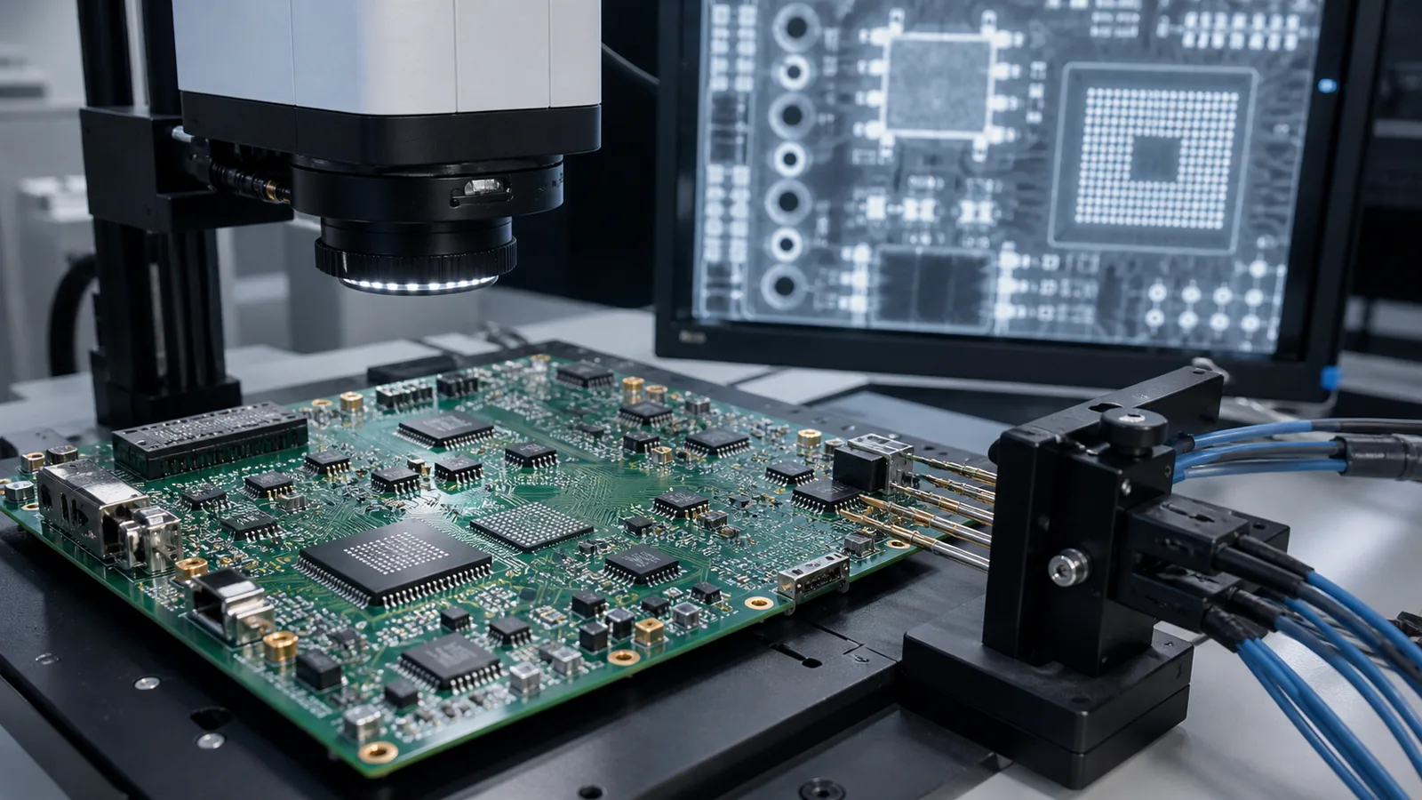
X-ray inspection creates an image from differences in material absorption so hidden solder joints and internal assembly structures can be evaluated. It is especially relevant to BGA, QFN, LGA, BTC, and other packages whose terminations are not fully visible from the exterior.
X-ray images may reveal hidden bridging, misalignment, uneven solder distribution, some open or poorly formed joints, and voiding. The evidence that can be extracted depends on package geometry, board construction, image angle, equipment configuration, and the inspection objective. A two-dimensional image can superimpose structures, while other imaging approaches may separate layers or views when justified.
X-ray inspection may be used or required depending on package type, process risk, customer requirements, and quality criteria. Not every BGA requires the same X-ray plan, and an image does not by itself define acceptance. Project criteria and engineering judgment determine whether an observed feature is acceptable, requires review, or calls for process correction. The BGA assembly and inspection guide covers hidden-joint considerations without expanding this comparison into a complete BGA tutorial.
In-Circuit Testing (ICT)
ICT uses electrical access to circuit nodes to check connectivity and selected component or network characteristics on an assembled board. A developed ICT strategy can detect shorts, opens, certain incorrect component values, and some presence or orientation errors that produce measurable electrical differences. It may also exercise basic node-level behavior, depending on the fixture and program.
Conventional ICT commonly requires accessible test points, a bed-of-nails fixture, and a test program matched to the released design. Coverage depends on board layout, probe access, component isolation, test-point distribution, fixture design, and the measurements included. Dense assemblies and limited test access can restrict what can be measured without design provisions.
ICT does not test every possible product function. It is strongest when the design, fixture, and coverage objectives are coordinated, particularly for stable production where repeatability can justify tooling. Test-point access is relevant here, but a complete design-for-test strategy belongs in a dedicated DFT review rather than this methods comparison.
Flying Probe Testing
Flying probe testing uses movable probes to contact selected electrical points without a dedicated bed-of-nails fixture. Bare-PCB flying probe testing checks unassembled board connectivity and isolation; assembled-board flying probe testing is a different application that may check selected PCBA nodes, component values, shorts, or opens when suitable access and programming are available.
For certain prototypes or low-volume assemblies, movable probes may provide electrical access with less dedicated fixture investment and greater flexibility after design changes. The tradeoff is typically longer test time, physical access constraints, and coverage that depends on the board and test strategy.
Flying probe is not simply another name for ICT, and not every PCBA supplier uses assembled-board flying probe testing. The supplier must confirm whether the assembly, access points, volume, and desired fault coverage fit the available method.
Functional Testing
Functional testing powers the PCBA and verifies whether it performs defined operations under specified test conditions. A procedure may check power rails, current draw, startup behavior, interfaces, I/O, communications, sensors, control responses, analog signals, protection behavior, or other product-specific outputs.
Functional coverage depends on the test specification. Development normally requires expected inputs and outputs, operating limits, connector definitions, power requirements, sequences, tolerances, pass/fail criteria, and failure-disposition rules. A fixture, cable harness, simulator, load, reference unit, or software interface may be needed to create repeatable conditions.
Functional testing verifies defined requirements; it does not guarantee field reliability or expose every workmanship defect. A procedure that checks only power-up cannot support a claim about every interface. Likewise, a comprehensive functional sequence does not replace inspection of soldering and assembly conditions that may matter to long-term performance.
Programming and Firmware Verification
Some projects require MCU or FPGA programming, firmware loading, configuration data, calibration constants, or serial-number programming before complete functional testing. Where required, the test record should identify the approved firmware version and programming result so a hardware failure is not confused with missing or incorrect software.
Not every PCBA needs programming. The customer should provide controlled files, device and interface information, security or serialization rules where applicable, and a method for verifying the programmed revision.
Which PCB Assembly Defects Can Each Method Detect?
The matrix below describes typical capability, not guaranteed fault coverage. “Strong” means the method commonly addresses the issue when correctly implemented; “Limited” means detection depends heavily on visibility, access, program, design, or procedure; and “Not typical” means another method normally provides more direct evidence.
| Defect or issue | Visual | AOI | X-ray | ICT | Functional test |
|---|---|---|---|---|---|
| Missing component | Strong when visible | Strong when visible | Limited | Limited | Limited |
| Wrong polarity or orientation | Strong when marked and visible | Strong when programmed and visible | Limited | Limited if electrically detectable | Limited |
| Component offset | Strong when visible | Strong when visible | Limited for hidden packages | Not typical | Limited |
| Visible solder bridge | Strong | Strong | Possible | Strong if it creates a measurable short | Limited |
| Hidden BGA bridge | Not typical | Not typical | Strong | Strong if electrically accessible | Limited |
| Open solder joint | Limited | Limited | Possible for hidden geometry | Strong where covered | Possible if the function exercises the path |
| Short circuit | Limited to visible bridges | Limited to visible bridges | Possible for hidden joints | Strong where covered | Possible, often after safe pre-power checks |
| Incorrect component value | Limited by markings | Limited by visible identification | Not typical | Strong for selected measurable parts | Possible if behavior changes |
| Insufficient visible solder | Strong | Strong when programmed | Limited | Limited | Limited |
| BGA voiding | Not typical | Not typical | Strong for imageable joints | Not typical | Not typical |
| Power-up failure | Not typical | Not typical | Not typical | Limited | Strong |
| Interface failure | Not typical | Not typical | Not typical | Limited | Strong when included |
| Firmware or function issue | Not typical | Not typical | Not typical | Not typical | Strong when included |
Prototype vs Production PCBA Testing
Prototype and production builds use the same inspection and testing principles but often balance flexibility, tooling, speed, and traceability differently. Prototype and low-volume work may emphasize engineering observation, accessible measurements, flexible harnesses, functional validation, and methods that tolerate design changes without extensive dedicated tooling. Flying probe or bench-level electrical checks may be considered where they fit the assembly and coverage objective.
Production testing often emphasizes repeatable AOI programs, stable fixtures, controlled software, practical cycle time, recorded pass/fail criteria, and consistent failure disposition. ICT may become more attractive when design stability, access, volume, and fault coverage justify fixture development. Functional fixtures may also be standardized for repeat builds.
These are tendencies, not fixed rules. A high-risk prototype may need X-ray and extensive functional validation, while a simple production board may not justify ICT. The selected combination should follow defect risk and acceptance needs rather than labels such as “prototype” or “mass production.”
How to Choose a PCB Assembly Test Plan
A PCB assembly test plan should be risk-based and project-specific. The planning team should identify likely defects, determine which evidence can reveal them, and define acceptance before production begins.
- Package visibility: Identify hidden terminations, shields, tall components, and dense areas that limit optical access.
- Board complexity: Consider node count, mixed technologies, analog and digital sections, power circuitry, and interface variety.
- BGA, QFN, or LGA presence: Decide whether package and process risk justify X-ray inspection.
- Electrical test access: Review accessible pads, connectors, test points, and isolation constraints.
- Production volume: Balance repeatability and cycle time against fixture and program development.
- Functional risk: Define which failures would affect safety, performance, integration, or customer acceptance.
- Acceptance requirements: Convert customer, regulatory, or product requirements into observable pass/fail criteria.
- Build stage: Account for engineering prototypes, pilot builds, stable production, and revision changes.
- Expected defect modes: Match visible, hidden, electrical, and functional risks to appropriate methods.
- Fixture economics: Consider fixture complexity, maintenance, revision exposure, and expected usage.
- Traceability: Define which serial number, firmware, measurement, image, or result records are required.
More testing does not automatically produce better quality. Useful coverage comes from selecting methods that address meaningful risks and controlling the resulting data. Fixture, programming, engineering, and cycle-time implications belong in the commercial scope; the PCB assembly cost breakdown explains those cost drivers in context.
Information Required From the Customer
A supplier needs controlled production data and measurable acceptance requirements to develop an appropriate PCBA inspection and testing plan. The starting package may include:
- Gerber or ODB++ production data and NC drill information
- BOM with manufacturer part numbers and approved alternatives
- Assembly drawing and polarity or orientation information
- Pick-and-place or centroid data
- Schematic where electrical or functional test development requires it
- Test specification and required measurements
- Functional requirements, operating sequence, and expected outputs
- Programming files and instructions where applicable
- Approved firmware version and configuration data
- Pass/fail criteria, limits, and failure-disposition instructions
- Connector, interface, power, load, and communications definitions
- Existing fixture or harness requirements, if already defined
- Prototype and production quantities
- Serial-number and traceability requirements where applicable
If the supplier is expected to develop a functional test, statements such as “test the board” are not sufficient. The customer must define intended behavior, controllable inputs, expected outputs, tolerances, operating conditions, and acceptance authority. The PCB production package checklist provides broader guidance for organizing released manufacturing and assembly inputs.
Common PCB Assembly Testing Mistakes
- Assuming AOI replaces electrical testing: optical evidence cannot establish every connection, value, or powered behavior.
- Assuming functional testing replaces workmanship inspection: a limited function can pass even when an unobserved assembly condition remains.
- Providing no practical test access: inaccessible nodes can reduce ICT or probing coverage and complicate debug.
- Using an incomplete functional specification: missing limits and expected outputs produce ambiguous results.
- Testing the wrong firmware revision: hardware can be misdiagnosed when software and configuration are uncontrolled.
- Leaving pass/fail criteria undefined: measurements without acceptance limits do not create a consistent quality decision.
- Changing the design without updating fixtures and programs: stale test assets can contact the wrong points or apply invalid criteria.
- Using one method for both visible and hidden defects: optical, X-ray, electrical, and functional evidence address different failure modes.
- Waiting until full production to validate the plan: pilot builds can reveal coverage, fixture, data, and cycle-time gaps earlier.
Excel Circuit can coordinate PCB inspection and testing support around the approved project scope. This educational comparison explains method selection; the service page defines available commercial support.
Frequently Asked Questions
What is the difference between AOI and ICT?
AOI uses optical imaging to inspect visible placement and solder features. ICT uses electrical access to check shorts, opens, selected component values, and other node-level conditions included in a developed test program. They address different evidence and may be used together.
Can AOI detect BGA solder defects?
AOI can inspect visible package placement and surrounding features, but it cannot directly see solder balls hidden beneath a BGA. X-ray inspection or electrical and functional evidence may be selected for hidden-joint risk depending on project requirements.
When is X-ray inspection needed for PCB assembly?
X-ray may be selected for BGA, QFN, LGA, and other bottom-terminated packages, or when process risk and customer criteria justify examination of hidden solder. It is not automatically required in the same form for every assembly.
Does every PCB assembly need functional testing?
No single functional procedure fits every PCBA. Functional testing is selected when defined product behavior must be verified, and its scope depends on risk, requirements, available fixtures, firmware, and acceptance criteria.
What information is required to develop a functional test?
The supplier typically needs the schematic where required, interface and connector definitions, power conditions, controllable inputs, expected outputs, tolerances, operating sequence, firmware, fixture responsibilities, and explicit pass/fail criteria.
Is ICT suitable for prototypes?
ICT can be used for prototypes when access, fixture, schedule, and coverage needs justify it, but dedicated tooling may be less attractive during frequent design changes. Flexible probing or functional debug may be considered instead; the decision is project-specific.
Request a PCBA Testing Review
Send your Gerber or ODB++ files, BOM, assembly data, quantities, and test requirements for a PCBA inspection and testing review. Excel Circuit can review package visibility, expected defect modes, test access, programming needs, functional criteria, and traceability requirements within a prototype-to-production assembly scope.