Stackup Engineering
Material, layer count, dielectric thickness and copper weights selected using a PCB stackup design guide, with your fabricator and performance targets in mind.

High-density interconnect design engineered for compact size, reliable signal performance and production-ready manufacturability.
More function in less space
HDI design is more than fitting smaller traces onto a board. We coordinate stackup, microvia structure, impedance, power integrity and BGA fan-out from the beginning—reducing redesign risk while improving density and electrical performance.
Core design capabilities
Material, layer count, dielectric thickness and copper weights selected using a PCB stackup design guide, with your fabricator and performance targets in mind.
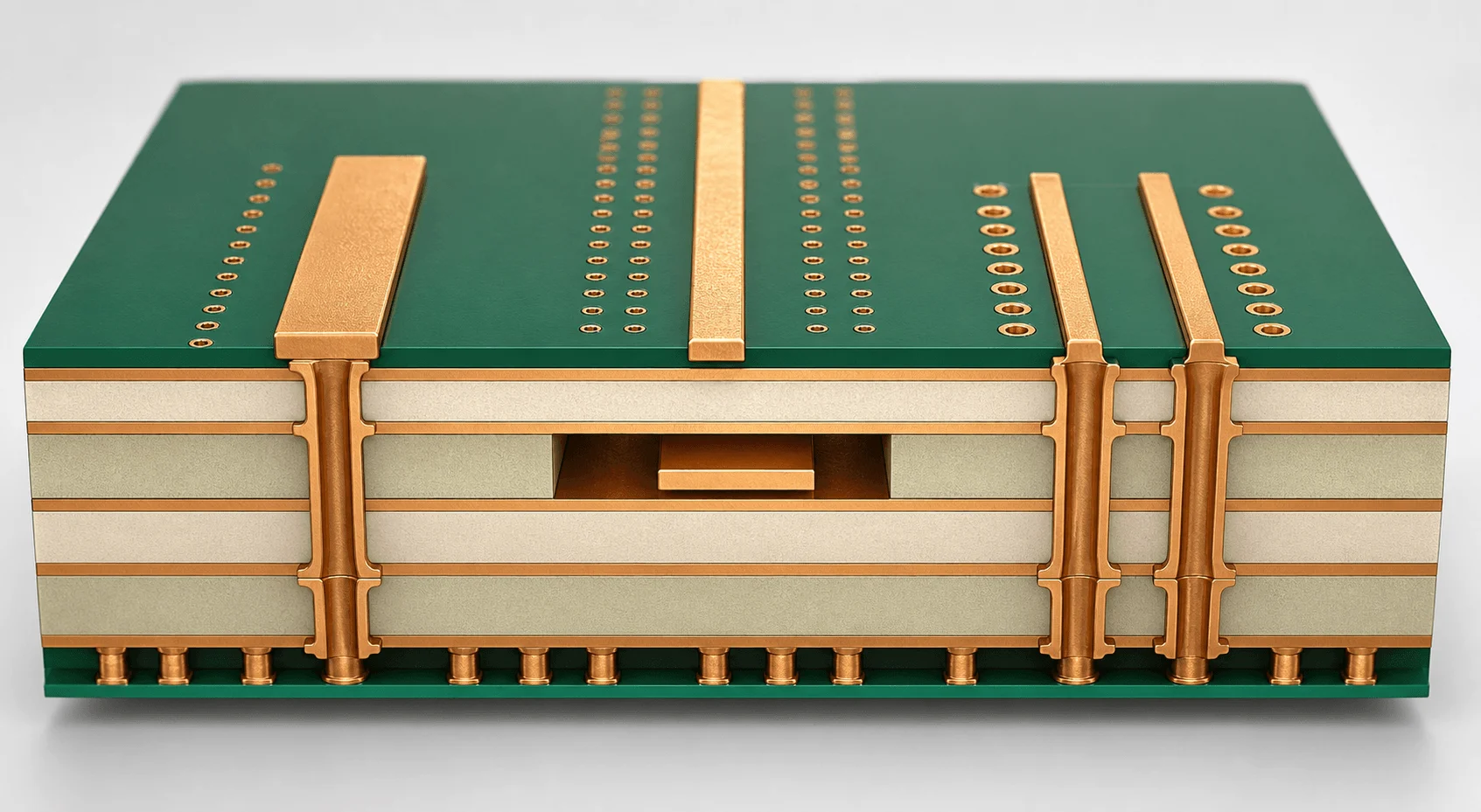
Stacked, staggered and via-in-pad structures planned for reliability, routing density and manufacturability.
Optimized escape routing for dense BGAs, CSPs and compact packages while protecting return paths.
Controlled impedance, reference-plane continuity and power distribution considered throughout placement and routing.
Clearance, annular ring, solder-mask, assembly access and fabrication constraints checked before release.
Gerber or ODB++, drill data, stackup, fabrication drawings and assembly files prepared for a clean handoff.
HDI structure options
The final structure is confirmed with the manufacturer according to board thickness, aspect ratio, reliability targets and cost.
HDI PCB design case studies
Each project begins with package geometry, mechanical limits and fabrication capability—then builds the stackup, microvia strategy and routing rules around those constraints.
 01Fine-pitch BGA
An HDI and fine-pitch BGA project combining processing, memory, power conversion and multiple high-speed interfaces.
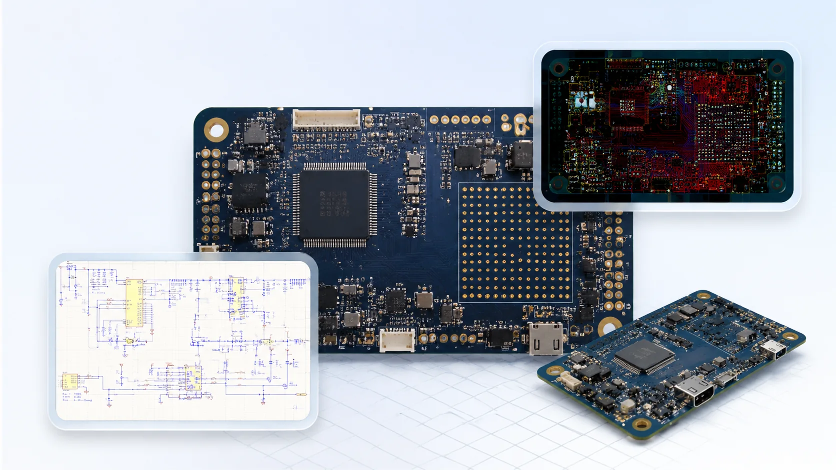 02Design workflow
A complete PCB development workflow translating system requirements and schematics into a dense, manufacturing-ready board design.
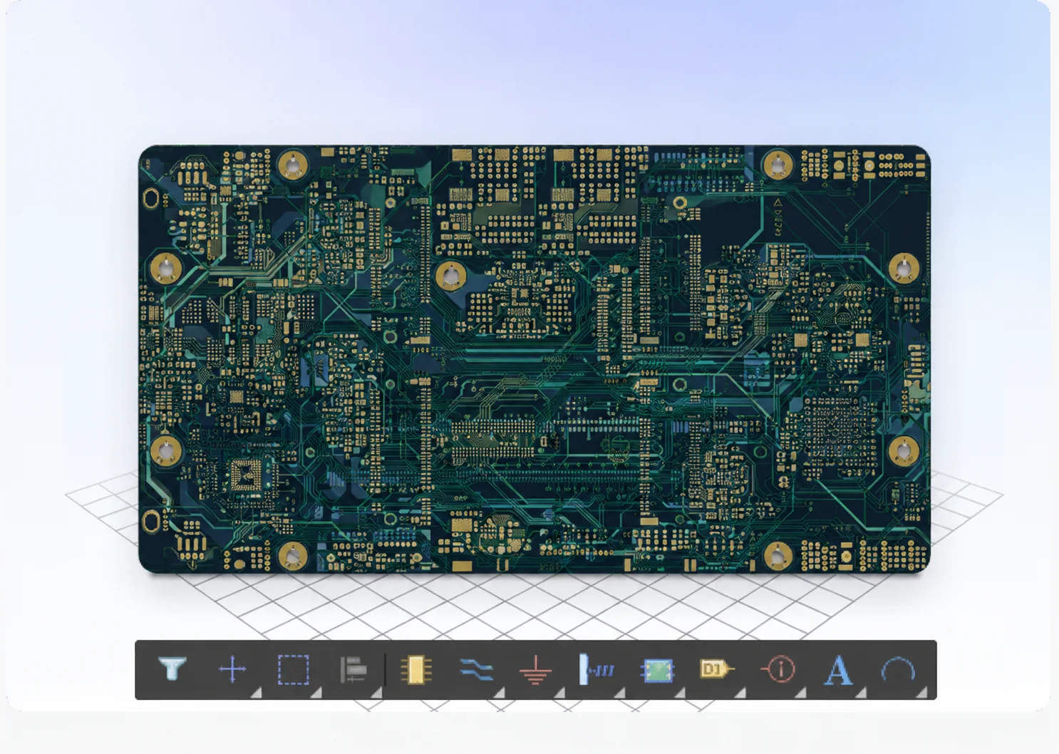 03Dense routing
A complex multilayer PCB layout with fine-pitch footprints, dense interconnects and tightly coordinated routing channels.
These examples illustrate representative project types and engineering approaches. Details are adapted to protect customer confidentiality.
Design workflow
Applications
Frequently asked questions
HDI is useful when fine-pitch components, limited board area, high interconnect density or electrical performance make conventional through-via routing impractical.
Yes. We can work with your approved fabricator or coordinate with Excel Circuit manufacturing so the design rules and released stackup match real production capability.
Please provide schematics, BOM, mechanical constraints, component datasheets, interface requirements and any preferred layer-count or impedance targets.
Purchasing FAQ
Practical answers about files, schedule, engineering support, production coordination and confidentiality.
Lead time depends on design maturity, complexity, quantity, material or component availability, testing scope, and how quickly engineering questions are resolved. We confirm the schedule after reviewing your files; urgent prototype or quick-turn options can be discussed where the required process and materials permit.
We can review common production outputs such as Gerber and ODB++, as well as native EDA data when agreed during the file review. Because library versions, third-party models and tool releases vary, tell us the software and version used before transfer so we can confirm the working format or recommend a neutral export.
Yes. SI/PI review or simulation can be included when the design contains high-speed interfaces, sensitive analog sections or demanding power rails. Scope depends on available stackup data, IBIS/SPICE models and measurable acceptance targets, so it is quoted separately when needed.
Project files are limited to personnel and qualified partners who need them for quotation and delivery. Excel Circuit uses reasonable technical and organizational safeguards, does not publish customer designs without permission, and can work under a mutually agreed NDA. Your signed NDA or project agreement controls where it provides specific protections.
Final scope, price and lead time are confirmed after engineering review of your current files and requirements.