
Contents
A reliable PCB does not begin with routing. It begins with clear inputs, an agreed design strategy and a repeatable review process. This guide turns a complex enterprise workflow into 22 practical steps—from the first schematic review to production-ready files.
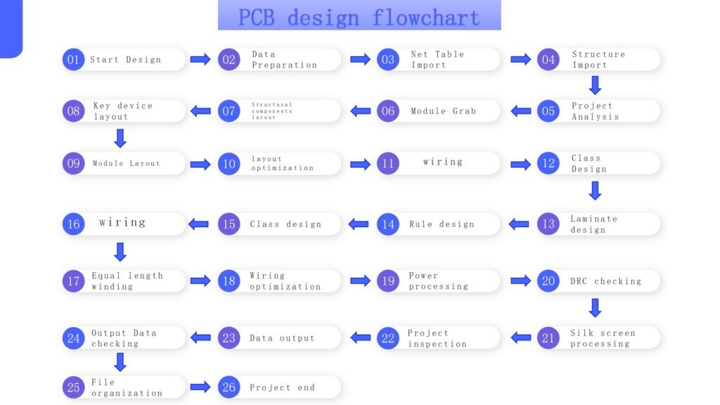
PCB design workflow at a glance
The process moves from understanding constraints to building the layout, validating the design and preparing controlled manufacturing data. Each phase has a clear output, so reviewers know when the design is ready to advance.
Inputs and project analysis
Establish the source of truth before placing a single component.
Prepare the design inputs
Collect and confirm the final project data:
- Approved schematic and all hierarchical pages
- Verified footprint library or component datasheets
- DXF board outline, connector locations and height limits
- Design notes covering critical signals, special IC requirements and fabrication limits
- Reference layouts and important device manuals
Import and verify the netlist
Import component packages and electrical connectivity from the latest schematic. Resolve missing footprints, pin mismatches and unexpected network changes before continuing.
Import the mechanical structure
Load the current board outline, mounting holes, keep-out areas and fixed component locations from the DXF file. Recheck the PCB whenever the enclosure changes.
Analyze the project
Build a functional block diagram, interpret design notes and map the power tree. Record voltage rails, current demand, signal direction and the interfaces between major modules.
Component planning and placement
Turn the project architecture into a logical, manufacturable physical layout.
Group functional modules
Group devices by function—power, processing, memory, RF, interfaces or analog circuitry. This makes signal flow visible and helps estimate the space each module requires.
Place mechanically constrained parts
Lock connectors, switches, LEDs, mounting holes and height-sensitive components to their approved locations. Confirm orientation and access from the enclosure.
Place key devices
Position the main ICs according to signal flow, thermal needs and interconnect density. A strong pre-layout reduces crossings and prevents one area of the board becoming overcrowded.
Complete the modular layout
Place supporting components around each main device. Follow datasheet recommendations for decoupling, crystals, feedback networks, RF matching and sensitive analog sections.
Optimize the layout
Review routing channels, return paths, component spacing, test access, assembly orientation and thermal distribution. Move parts now—before traces make changes expensive.
Stack-up, constraints and routing
Translate electrical and manufacturing requirements into enforceable PCB rules.
Define the layer stack-up
Estimate the required layer count from routing density, power distribution and reference-plane needs. Confirm board thickness, copper weight, dielectric materials and impedance geometry with the PCB manufacturer.
Set fabrication rules
Configure minimum trace width, spacing, via sizes, annular rings and copper clearances. Rules must satisfy both product requirements and the selected fabrication process.
Create signal classes
Group networks with shared requirements, such as differential pairs, clocks, memory buses, high-current rails and sensitive analog signals. Assign the correct width, spacing, impedance and length constraints.
Route by priority
Route critical signals first, then power-sensitive and timing-sensitive groups, followed by general signals. Maintain continuous reference planes and avoid unnecessary layer transitions.
Apply length matching
Match timing-critical traces within the tolerance defined by the interface or IC vendor. Tune with controlled geometry and avoid excessive serpentine coupling.
Optimize routing
Review key nets for short paths, clean return-current flow, reasonable via count, smooth fan-out and sufficient separation from noisy circuitry.
Complete power processing
Create power and ground planes, copper pours and transitions sized for current and thermal requirements. Do not split a reference plane beneath a critical signal path.
Verification and design release
Check connectivity, manufacturability and documentation before generating final files.
Run DRC and connectivity checks
Confirm that every required network is connected and that there are no shorts, unconnected pins, clearance violations, keep-out intrusions or prohibited component placements.
Finish the silkscreen
Place readable reference designators, polarity marks, pin-one indicators, revision data, serial-number areas, logos and required safety or ESD markings. Keep text clear of pads and exposed copper.
Perform the final project review
Review the design against the schematic, mechanical constraints, customer requirements and manufacturing notes. A checklist-based peer review is more reliable than memory.
Generate and inspect Gerber data
Output the Gerber or ODB++ package, drill files, IPC netlist and fabrication drawings. Open the exported files in an independent viewer and perform a DFM check before release.
File release and controlled archiving
Make the design easy to manufacture, revise and trace later.
Release the manufacturing package
Send only reviewed and revision-controlled files. Include a fabrication drawing, stack-up, impedance table, drill data, netlist and special process notes. For assembly, add the BOM, centroid data and assembly drawings.
Archive the project
Store source and output data in a consistent folder structure. Record the revision, release date, reviewer and any approved deviations so future updates begin from the correct baseline.
Recommended project folder structure
| Folder | Recommended contents | Primary recipient |
|---|---|---|
| ASM | Top and bottom assembly drawings and assembly notes | PCBA / assembly team |
| CAM | Gerber or ODB++, drill data, IPC netlist and fabrication instructions | PCB manufacturer |
| DXF | Approved board outline and mechanical reference files | Mechanical engineer |
| PCB | Final native PCB layout files and libraries | PCB design team |
| SCH | Final schematic source, PDFs and library references | Hardware engineering team |
| SMT | BOM, centroid data, stencil data and placement instructions | SMT factory |
Final release checklist
- Schematic revision matches the PCB revision
- Board outline and mounting locations are approved
- Footprints and polarity are verified
- Stack-up and impedance are confirmed by the fabricator
- Critical trace widths, spacing and lengths pass checks
- Power paths meet current and thermal requirements
- No critical trace crosses a reference-plane split
- DRC and connectivity checks show no unexplained errors
- Silkscreen is readable and clear of solderable areas
- Gerber, drill and netlist files pass independent review
- BOM, centroid and assembly drawings share one revision
- The released package is archived with approval records
Need a second set of engineering eyes?
Excel Circuit can support schematic review, PCB layout, stack-up planning, DFM checks, fabrication and assembly—helping you move from design requirements to a production-ready board with fewer late-stage surprises.
Discuss your PCB project