Contents
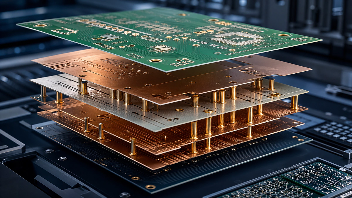
A printed circuit board is a layered electrical and mechanical structure that supports components and connects them through patterned copper conductors. Its performance depends on the substrate, copper layers, dielectric construction, holes and vias, solder mask, surface finish, geometry, and manufacturing quality.
Core, Prepreg, and Substrate Materials
A core is a cured laminate with copper on one or both sides. Prepreg is resin-impregnated reinforcement used to bond layers during lamination. FR-4 is common, but high-frequency, high-temperature, flexible, metal-core, and ceramic materials serve different electrical, thermal, and mechanical requirements.
Copper Layers and Reference Planes
Signal layers carry routed nets, while ground and power planes provide references, return-current paths, shielding, and power distribution. Copper thickness and finished geometry affect resistance, current capacity, impedance, etching, and manufacturability.
Plated Holes and Vias
Through vias connect layers through the full board. Blind and buried vias connect selected layers, while microvias are typically laser formed for HDI structures. Pad size, drill size, aspect ratio, plating, layer span, and reliability limits depend on the qualified fabrication process.
Solder Mask and Silkscreen
Solder mask protects copper and controls solderable openings, but it is not a universal electrical-insulation barrier. Silkscreen communicates reference designators, polarity, warnings, and assembly information and must not cover pads or critical features.
Surface Finishes
A surface finish protects exposed copper and provides a solderable or contact surface. ENIG, immersion silver, immersion tin, HASL, OSP, and other finishes differ in flatness, shelf life, cost, assembly compatibility, and application limits.
How Multilayer PCBs Are Built
Multilayer boards are imaged, etched, aligned, laminated, drilled, plated, coated, finished, profiled, tested, and inspected through a process adapted to the chosen construction. See the PCB manufacturing process guide.
Structure Selection Checklist
Define layer count, board thickness, material, copper, impedance, via technology, minimum features, finish, environment, thermal needs, assembly process, and test requirements before release.