Contents
Before sending a PCB design for manufacturing, verify that the fabrication package contains the correct copper, solder mask, silkscreen, board outline and NC drill data. Confirm that the PCB revision, layer stackup, hole types, copper requirements, surface finish, controlled impedance and any special via or fabrication instructions match the intended production release. The exact package can vary with board complexity and project requirements. Excel Circuit’s PCB manufacturing services can review the available fabrication data against the requested build.
Quick Gerber File Checklist
Use this checklist to compare the exported manufacturing data with the approved PCB revision. Some items apply only to particular board structures or project requirements.
| Item | What to Verify | Common Issue |
|---|---|---|
| Top / Bottom Copper | Correct copper data for both external layers. | Missing or outdated layer file. |
| Internal Copper Layers | All internal signal and plane layers are included in the correct order. | Incorrect layer order or missing inner layer. |
| Solder Mask | Top and bottom solder mask data matches the intended pad and exposed-copper openings. | Missing mask layer or unintended openings. |
| Silkscreen | Correct top and bottom legend data, reference designators and polarity marks. | Silkscreen overlapping pads or a wrong-side legend. |
| Board Outline | A clear and unambiguous finished board profile is included. | Multiple conflicting outlines or missing cutouts. |
| NC Drill Files | Drill data uses the intended units, origin and hole definitions. | Missing drill file or coordinate mismatch. |
| Plated / Non-Plated Holes | PTH, NPTH, slots and mechanical holes are clearly identified. | Incorrect plating definition. |
| Fabrication Notes | Special manufacturing requirements are documented where required. | Critical requirements exist only in email or design notes. |
| Stackup Information | Layer order, board thickness and relevant material requirements are identified. | Gerber layer names do not clearly define the stack order. |
| Controlled Impedance Requirements | Target impedance and applicable nets or layers are identified where required. | Impedance requirements are missing from the fabrication package. |
| Copper Thickness | Required copper weight or finished-copper requirement is clear. | Outer and inner copper assumptions differ from the design intent. |
| Surface Finish | The required finish, such as ENIG, HASL or another project-specific finish, is stated. | Surface finish is omitted from quotation data. |
| Special Via Requirements | Blind, buried, microvia or via-in-pad requirements are identified. | Special via construction is not communicated to the manufacturer. |
1. Verify All Copper Layers
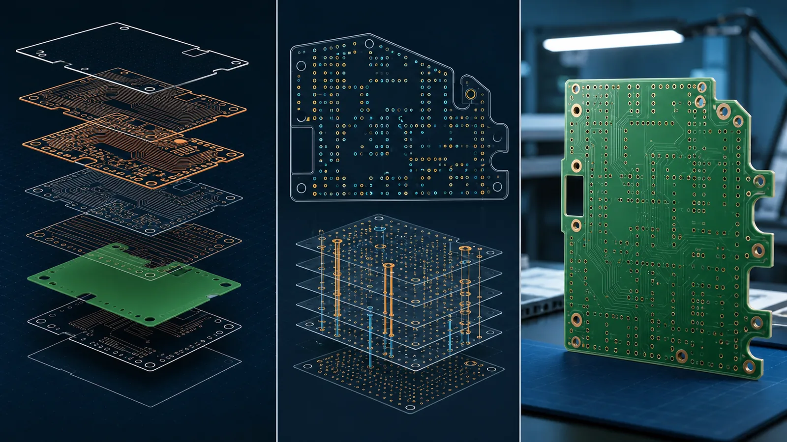
Copper output defines the conductive geometry used to manufacture the board. Compare every exported copper layer with the approved PCB revision rather than assuming that a successful export includes the intended data. Check the two external copper layers and, for a multilayer PCB, every internal signal and plane layer.
Top and Bottom Copper
Confirm that the top and bottom copper files contain the expected pads, traces, pours and other conductive features. The files should belong to the current board revision and use a naming convention that does not confuse the two sides. Review the exported data in a Gerber or CAM viewer where practical, because the manufacturing output—not only the view inside the PCB CAD editor—is what the manufacturer receives.
Internal Signal and Plane Layers
For multilayer designs, verify that all internal signal and plane data is present. Confirm whether each internal layer is a routed signal layer, a solid reference plane or a mixed layer. Positive and negative image polarity should be identified where applicable, particularly when plane-layer output could otherwise be interpreted incorrectly.
Layer Naming and Order
Gerber file names alone should not be relied upon when the stackup is ambiguous. Names such as “inner1” or “plane2” do not necessarily establish the physical sequence. Provide or reference clear stackup information so the manufacturer can determine the intended order from the top side to the bottom side. Before release, compare that sequence with the fabrication notes and controlled-impedance information to make sure they describe the same revision.
2. Check Solder Mask Layers
Solder mask files define where the mask remains and where copper is intentionally exposed. Confirm that both top and bottom mask outputs are included when both sides require mask processing. The exported openings should match the intended component pads, test points, edge contacts and other exposed-copper features.
Solder Mask Openings
Inspect pad openings around fine-pitch components, through-hole pads, vias and connectors. Look for unintended openings, missing openings and mask clearances that do not match the released design. Where mask-defined pads or other mask-controlled features are used, identify them clearly in the fabrication data or notes so their purpose is not mistaken for an export error.
Exposed Copper Areas
Review intentional exposed copper such as grounding areas, contact surfaces, heat-spreading regions or edge features. Confirm that these areas appear correctly in the final manufacturing output. A correct display in the PCB CAD editor does not guarantee that the generated mask files contain the same geometry, so the exported layers should be checked independently before release.
3. Check Silkscreen Layers
Silkscreen provides assembly, inspection and service information on the finished board. Confirm that the correct top and bottom legend layers are included for the approved revision. Reference designators, polarity marks, pin 1 indicators, connector labels and warning text should correspond to the actual component placement and board orientation.
Inspect the exported legend for text or graphics placed over solderable pads, exposed copper or openings. These elements may be clipped or removed during manufacturing according to manufacturer-specific clearance rules. Moving critical polarity or orientation information away from restricted areas can make the final marking more reliable and readable.
Check that text is readable at the intended size and is not mirrored, placed on the wrong side or obscured by components. If bottom-side text is intentionally mirrored in the CAD workflow, confirm that the exported output matches the manufacturer’s expected viewing convention. Nonessential design notes should not be mixed with production legend data where they could create uncertainty.
4. Verify Board Outline
The fabrication package should identify one clear finished board profile. Confirm that the outline forms the intended closed contour and includes the correct overall dimensions, corners, notches and other edge geometry. Internal cutouts, routed slots and edge-routing features should be represented in a way that can be distinguished from documentation lines.
If several mechanical layers contain outlines, dimensions, keep-out boundaries or enclosure references, make it clear which geometry defines the finished board profile. Multiple overlapping or slightly different contours can create uncertainty about the intended routing path. Fabrication notes or a drawing can clarify which mechanical data is authoritative.
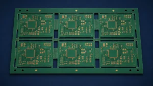
Also distinguish an individual-board outline from panel rails, breakaway tabs, tooling borders or other panel-related geometry. If the submitted data represents a customer-designed panel, label the panel and unit profiles clearly. If only the individual PCB is being released, avoid leaving obsolete panel or mechanical outlines in the manufacturing package. This establishes the intended profile without attempting to define a complete panelization method.
5. Include NC Drill Files
Gerber copper data does not replace NC drill information. The drill output identifies the locations and definitions of round holes, and separate routing data may be required for slots or other machined features depending on the CAD and manufacturer workflow. Confirm that the released drill data belongs to the same PCB revision as the Gerber layers.
Drill Units and Coordinates
Check the selected units, numeric format and coordinate origin. Gerber and drill data should align when loaded together in a CAM viewer. A unit, zero-suppression or origin mismatch can shift hole locations or change their scale even when each individual file appears syntactically valid. Include the drill format information generated by the selected CAD workflow where it helps remove ambiguity.
PTH and NPTH Data
Identify plated through holes and non-plated holes clearly. Separate PTH and NPTH outputs may be used, but the exact export arrangement can differ between CAD systems and manufacturer workflows. Mechanical holes, press-fit holes, slots and routed features should carry sufficient information for their intended plating and finished geometry to be understood.
Before release, load the copper, outline and drill data together and check registration around pads, mounting holes and cutouts. Confirm that no obsolete drill file remains in the package and that any routing data required for non-round features is included where applicable.
6. Confirm Plated and Non-Plated Holes
Hole data should communicate both geometry and plating intent. Plated through holes (PTH) create an electrical or mechanical connection through the board, while non-plated through holes (NPTH) are commonly used for mounting, tooling or other mechanical functions. Slots and elongated holes also need a clear definition because their manufacturing method may differ from that of round drilled holes.
PTH vs NPTH
PTH and NPTH must be clearly distinguishable in the fabrication data, whether by separate drill files, attributes, fabrication notes or another manufacturer-accepted method. They do not necessarily have to be exported as separate files in every CAD or CAM workflow. Confirm that mounting holes, component holes, press-fit features, plated slots and non-plated slots carry the intended definition. If a mechanical hole is close to copper, also verify that its plating status and surrounding clearance agree with the released design.
Finished Hole Size and Drill Size
Finished hole size and drill tool size are not always identical. Plated holes receive copper and other process layers on the barrel, so the production drill size may include an allowance for the intended finished opening. The appropriate allowance depends on the manufacturing process and should not be assumed as one fixed value. State the required finished hole size where it is critical, and coordinate drill interpretation with the manufacturer. Review drill tables, fabrication drawings and Gerber pad geometry together so that hole sizes, annular rings, slots and plating notes describe the same approved revision.
7. Provide Stackup Information
Gerber files describe layer artwork, but they do not by themselves fully communicate every physical stackup requirement. The fabrication package should make the intended layer sequence clear and identify the target finished board thickness, relevant copper requirements and the function of signal and plane layers.
Layer Order and Board Thickness
List the layer sequence from top to bottom so internal Gerber data cannot be assembled in the wrong order. Identify which internal layers are signals, reference planes, power planes or mixed layers. State the finished board thickness and any project-specific copper distribution. Where core, prepreg or laminate information is already defined, include it in the controlled fabrication documentation. Material family or laminate requirements should also be identified where electrical, thermal, mechanical or qualification needs make them relevant.
When Detailed Stackup Information Matters
For a conventional project, the manufacturer may propose a production stackup based on the target board thickness, copper thickness, available materials and process capability. This does not mean the customer has to define every core and prepreg thickness before requesting a quotation. The proposed construction should still be reviewed against the design intent before production.
Detailed coordination becomes more important for high-speed digital, controlled-impedance, RF, HDI, heavy-copper or mechanically sensitive designs. In those cases, dielectric thickness, material properties, copper distribution, reference-plane placement and via structure can affect electrical performance and manufacturability. Confirm the final production stackup before release, and make sure the PCB design rules, impedance requirements and fabrication drawing refer to the same stackup revision.
8. Specify Controlled Impedance Requirements
Controlled impedance requirements should be stated explicitly when they apply. Trace geometry visible in Gerber artwork does not automatically tell the manufacturer which conductors require impedance control, what the target value is or how the traces relate to the intended production stackup. This information is particularly relevant to high-speed digital interfaces, RF paths and differential interfaces.
Identify the Controlled Nets
Document whether each requirement is single-ended or differential, the target impedance and any project-defined tolerance where applicable. Identify the affected nets or net classes and the layers on which they are routed. Fabrication notes, an impedance table or other controlled documentation can be used, provided the manufacturer can relate the requirement to the correct traces, layer and revision. Avoid relying only on a generic statement such as “controlled impedance required” without identifying the relevant structures.
Coordinate Impedance with the Production Stackup
Impedance depends on trace geometry, finished copper, dielectric properties, dielectric thickness and the location of the reference plane. Coordinate the targets with the final production stackup rather than assuming that nominal CAD geometry will remain unchanged. If the manufacturer proposes a stackup or material adjustment, review any resulting trace-width or spacing changes before production. Tolerance, coupon and reporting requirements should follow the project specification or an agreement with the manufacturer; they should not be inferred from an arbitrary default.
9. Confirm Copper Thickness and Surface Finish
Copper and surface-finish requirements affect the physical board but are not fully defined by Gerber artwork. State them in the quotation or fabrication requirements so the manufacturer can evaluate the requested construction and process.
Copper Thickness
Identify the project-specific copper requirement for outer and inner layers. If different layers use different copper weights, document the distribution clearly. Heavy copper or other special copper requirements should be highlighted because they can affect etching, spacing, plating, lamination and the available stackup.
Where relevant, distinguish starting copper from finished copper. Nominal copper weight and finished copper thickness are related, but processes such as plating can affect the final result, particularly on outer layers. Avoid treating a nominal foil value as an exact universal finished thickness. Critical electrical, thermal or mechanical requirements should be expressed in the project documentation and coordinated with the selected manufacturing process.
Surface Finish
Specify the intended surface finish, such as ENIG, HASL, lead-free HASL, OSP or another project-specific finish where applicable. The appropriate selection depends on component, assembly, shelf-life, contact, environmental and project requirements; no single finish is universally best.
Surface finish should be stated in the quotation or fabrication requirements rather than assumed from the Gerber data. If selective finishes, edge contacts or special exposed-copper areas are involved, identify them through clear fabrication documentation. Confirm that the stated finish agrees with solder-mask openings, connector requirements and the released board revision.
10. Document Blind, Buried and Via-in-Pad Requirements
Special via structures require more information than a set of copper images and a generic drill table. Document the layers connected by each via type and any project-specific filling, capping, plating or sequential-lamination requirement. The manufacturer should be able to distinguish through vias from blind vias, buried vias, microvias and via-in-pad structures.
Blind and Buried Via Layer Pairs
A blind via connects an external layer to one or more internal layers, while a buried via connects internal layers without reaching either external surface. Identify the start and stop layer for each structure. If the design requires more than one lamination stage, document the intended build sequence or coordinate it with the manufacturer so the released stackup and drill data describe the same construction.
Via-in-Pad Requirements
Via-in-pad places a via within a component or feature pad, but that placement alone does not define the required finishing process. When filling or capping is required by the assembly or design process, that requirement should be explicitly documented. Identify whether the finished pad needs a particular surface condition or plating result, and ensure that the fabrication and assembly data refer to the same via-in-pad intent.
Microvia and Sequential Lamination Information
A blind via is defined by the layers it connects, while a microvia generally refers to a small via structure produced using a specific HDI process. The terms are related but not interchangeable. Identify microvia layer pairs and indicate stacked or staggered arrangements where they are part of the approved design. Coordinate filling, copper plating and sequential-lamination needs with the production stackup rather than assuming that all blind structures use the same process.
Common Gerber File Mistakes Before PCB Manufacturing
Many Gerber problems arise not because the CAD data cannot be generated, but because the release package contains inconsistent revisions, coordinates, layer definitions or manufacturing requirements.
| Mistake | Why It Matters | What to Check |
|---|---|---|
| Missing board outline | The manufacturer cannot reliably determine the intended finished profile. | Confirm one clear finished board outline and identify cutouts or routed features. |
| Missing drill data | Copper artwork alone does not define the complete hole pattern. | Confirm the intended drill or routing data is included. |
| Wrong layer polarity | Plane or negative-image interpretation can create incorrect copper. | Verify output polarity and layer interpretation before release. |
| Incorrect units or coordinate format | Gerber and drill data can become misaligned or incorrectly interpreted. | Verify units, format and origin across the released fabrication data. |
| Drill origin mismatch | Hole locations may not align with copper features. | Load Gerber and drill files together in a CAM or Gerber viewer. |
| Missing mechanical information | Slots, cutouts, bevels or other mechanical requirements may be unclear. | Include fabrication notes or clearly identified mechanical data where required. |
| Missing impedance requirements | The manufacturer may not know which nets or layers require impedance control. | Provide target impedance and applicable net or layer information. |
| Outdated fabrication files | A previous revision can accidentally enter production. | Regenerate and archive a single controlled release package from the approved design revision. |
| Gerber and drill files from different revisions | Copper, holes and mechanical data may no longer match. | Confirm all released manufacturing data comes from the same approved revision. |
Before release, export Gerber files from Altium or the applicable CAD tool, then load the exported Gerber and drill files into an independent Gerber or CAM viewer and inspect the manufacturing output rather than relying only on the PCB editor view. After validation, prepare a complete PCB manufacturing file package with the Gerbers and remaining production data.
If a release problem originates in the layout, stackup or source manufacturing data, the controlled correction should be made in the source design before regenerating the fabrication package. Excel Circuit’s PCB design and layout services can support design updates and production-ready data preparation.
Need an Engineering Review Before Production?
If you are unsure whether the fabrication package is complete, send the Gerber, drill and project files currently available. Our team can review the available manufacturing data before quotation and identify items that may need clarification.
Gerber Files vs Assembly Files
PCB fabrication data and PCBA assembly data serve different production stages. Fabrication files define the bare board, while assembly files identify the components, placement and instructions needed to build the populated assembly.
| File | PCB Manufacturing | PCB Assembly |
|---|---|---|
| Gerber / ODB++ | Core fabrication data. | Often used as reference where required. |
| NC Drill | Primary hole and routing input. | Normally not a primary assembly input. |
| Fabrication Notes | Used where applicable to define manufacturing requirements. | Reference only where relevant. |
| Stackup Information | Used where required to define the board construction. | Usually reference information. |
| BOM | Normally not required for bare PCB fabrication. | Key assembly and component-sourcing input. |
| Pick & Place | Not normally a fabrication input. | Primary SMT placement data. |
| Assembly Drawing | Not normally a fabrication input. | Used where required for component orientation and assembly instructions. |
A bare PCB manufacturing quotation typically focuses on fabrication data and board requirements, while a turnkey PCBA project may also require a BOM, pick-and-place data and assembly information. For projects that continue beyond bare PCB fabrication, see our turnkey PCB assembly service for component sourcing, SMT assembly and inspection support. The exact assembly package depends on the project stage and requirements.
What Should I Send for a PCB Manufacturing Quote?
When preparing Gerber files for PCB manufacturing, send the fabrication data currently available together with the board quantity and key production requirements. The exact package depends on board complexity, but providing clear PCB manufacturing files and specifications helps reduce clarification cycles before quotation and production. Information can be added or confirmed as the project becomes more defined.
- Available Gerber or ODB++ Data: Provide the current fabrication data generated from the approved PCB design revision.
- NC Drill Data: Include the available drill information for plated, non-plated and routed features where applicable.
- Board Quantity: Specify the prototype, pilot or production quantity required for quotation.
- PCB Material: State the required material family or laminate requirement where the project specifies one. A specific brand does not need to be assumed for every project.
- Finished Board Thickness: Provide the required finished thickness where it is defined by the design.
- Copper Requirement: State the required copper weight or finished-copper requirements where applicable.
- Surface Finish: Specify ENIG, lead-free HASL, OSP or another required finish where applicable.
- Controlled Impedance: Identify the target impedance and relevant layers or nets when impedance control is required.
- Special Process Requirements: Identify applicable blind or buried vias, via-in-pad, edge plating, controlled-depth routing or special mechanical requirements.
- Required Schedule: Provide the requested delivery date or project timing so the quotation can account for schedule requirements.
Frequently Asked Questions
What Gerber files are required for PCB manufacturing?
A common fabrication package includes copper layers, top and bottom solder mask, applicable silkscreen or legend layers, a clear board outline and NC drill data. Multilayer or technically sensitive designs may also need stackup information, controlled-impedance requirements, fabrication notes and special via instructions. The exact set depends on the board design, the selected output format and the manufacturer’s CAM workflow. Before submission, verify that the files belong to the same approved revision and that their layer functions can be identified without relying on ambiguous file names.
Do PCB manufacturers need NC drill files?
Bare PCB fabrication normally requires clear hole and drill information. Gerber copper artwork does not fully define plated holes, non-plated holes, slots and other machined features. NC drill data, or equivalent manufacturer-accepted drill data, communicates those locations and definitions. The information may be organized differently depending on the CAD export and manufacturer workflow, so a separate Excellon file should not be treated as the only possible arrangement. The important requirement is that drill units, origin, plating intent and routing information can be interpreted and aligned with the fabrication layers.
Do I need to provide the PCB stackup?
For a conventional PCB, the manufacturer may propose a production stackup based on the target finished thickness, copper requirements, available materials and process capability. The customer does not necessarily need to define every core and prepreg thickness before quotation. For high-speed, impedance-controlled, RF, HDI or otherwise sensitive designs, stackup agreement becomes more important because dielectric dimensions, material properties, reference planes and via construction affect performance. In those projects, confirm the production stackup and any related design-rule or impedance adjustments before manufacturing begins.
What is the difference between Gerber and ODB++?
Gerber commonly represents PCB fabrication as multiple layer-artwork files accompanied by NC drill files and supporting fabrication data. ODB++ is a more integrated data format that can contain layer information, drill data, net information and additional design or manufacturing attributes in one structured package. ODB++ does not universally replace Gerber, and neither format is inherently the best choice for every project. The appropriate format depends on the design-tool export, the information that needs to be transferred and the formats accepted by the manufacturer’s workflow.
Do I need a BOM for bare PCB manufacturing?
Usually no. A bill of materials is primarily used for component sourcing and PCB assembly rather than fabrication of the bare board. A bare PCB quotation normally focuses on the fabrication data, board specifications, quantity, schedule and special manufacturing requirements. A BOM becomes relevant when the project includes component procurement, assembly or other work beyond bare-board production. If a project will proceed through assembly, provide the BOM with the applicable placement and assembly information, but do not assume that the same package is needed for a fabrication-only quotation.
Can a PCB manufacturer review Gerber files before production?
Many PCB manufacturing workflows include an engineering or CAM review before production, although the scope varies by supplier and project. The review may identify missing files, unclear layer definitions, Gerber and drill mismatches or fabrication requirements that need clarification. It does not guarantee manufacturability or catch every electrical, mechanical or design error. CAM preparation, manufacturing-data review, PCB design-rule verification and overall engineering responsibility are related but different checks. Confirm what the supplier reviews and resolve open technical questions before approving the production data.
Ready for PCB Manufacturing?
Send your available Gerber files, drill data and project requirements for quotation. If your project will continue through component sourcing and assembly, you can also include BOM and assembly data with the RFQ.