Contents
Introduction
In power electronics PCB design, a high-current PCB must deliver power with acceptable voltage drop, temperature rise, electromagnetic behavior, safety margin, and manufacturing yield. That requires more than widening a few traces. Current moves through component leads, pads, neck-downs, pours, planes, vias, connectors, copper interfaces, and return paths; the weakest transition can dominate loss and heating.
The correct geometry depends on current waveform, duty cycle, allowable temperature rise, ambient and enclosure conditions, copper thickness, PCB stack-up, cooling, material limits, reliability target, and fabricator capability. Trace width, via count, clearance, and copper weight therefore must be calculated and verified for the actual project rather than copied from a universal chart.
Engineering Summary
- Map the complete outgoing and return-current paths before detailed placement.
- Size copper from loss and temperature-rise objectives using the real stack-up and cooling environment.
- Eliminate bottlenecks at pads, vias, fuses, shunts, connectors, and layer transitions.
- Keep switching loops compact and separate high-dv/dt and high-di/dt nodes from sensitive circuits.
- Coordinate heavy copper, clearances, thermal strategy, assembly, and DFM with the manufacturer.
Key Design Factors
Current waveform and operating modes
Continuous current, pulse current, startup surge, fault current, switching ripple, and regenerative current create different electrical and thermal stresses. Define RMS, peak, duration, repetition, duty cycle, and credible fault conditions. A route that survives a short peak may still fail a sustained thermal requirement, while a low average current can create severe localized switching loss.
Allowable voltage drop and temperature rise
Allocate the voltage-drop budget across connectors, protection devices, copper, vias, shunts, and component interfaces. Define the temperature limit at the copper, laminate, components, and enclosure—not only an abstract trace-rise target. Thermal performance depends on heat spreading into planes, convection, conduction to chassis, neighboring heat sources, and board orientation.
Safety and insulation
High current does not automatically mean high voltage, but power-electronics boards often include both. Creepage and clearance are determined by working voltage, transient category, pollution degree, material group, altitude, coating, applicable standard, and safety architecture. Use the requirements governing the actual product; do not apply a single spacing value to all designs.
Detailed Engineering Guidelines
1. Draw the complete power-current map
Trace each power loop from source through protection, switching devices, energy storage, load, and return. Include startup and fault paths, gate-drive returns, current-sense paths, and chassis or shield connections. Mark current direction and magnitude by operating state. This exposes shared copper, narrow transitions, and unintended return coupling before placement.
2. Place power devices around loop geometry
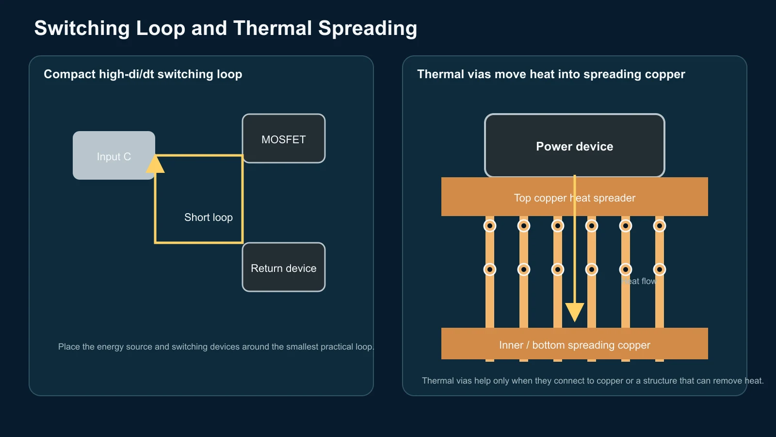
Place switching devices, input and output capacitors, magnetics, rectifiers, shunts, and connectors to minimize the electrically critical loops. The high-di/dt commutation loop should be compact and direct. Keep high-dv/dt switch-node copper no larger than necessary and away from control, feedback, clocks, and communication interfaces. Placement should also preserve realistic heatsinking, assembly, and service access.
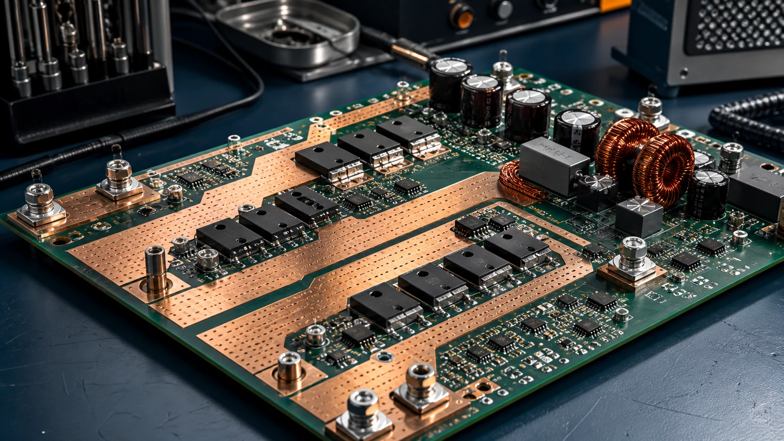
A power electronics board case study shows how current paths, switching loops, thermal constraints, and production requirements interact.
3. Size traces and pours from project conditions
Calculate resistance using finished copper geometry and temperature-dependent resistivity, then evaluate voltage drop and power loss. Estimate temperature rise with a method appropriate to the geometry and validate high-risk regions with thermal analysis or measurement. External and internal copper dissipate heat differently. Trace width cannot be selected from current alone; copper thickness, length, neighboring copper, airflow, duty cycle, laminate, and allowed temperature all matter.
4. Prefer broad, continuous current paths
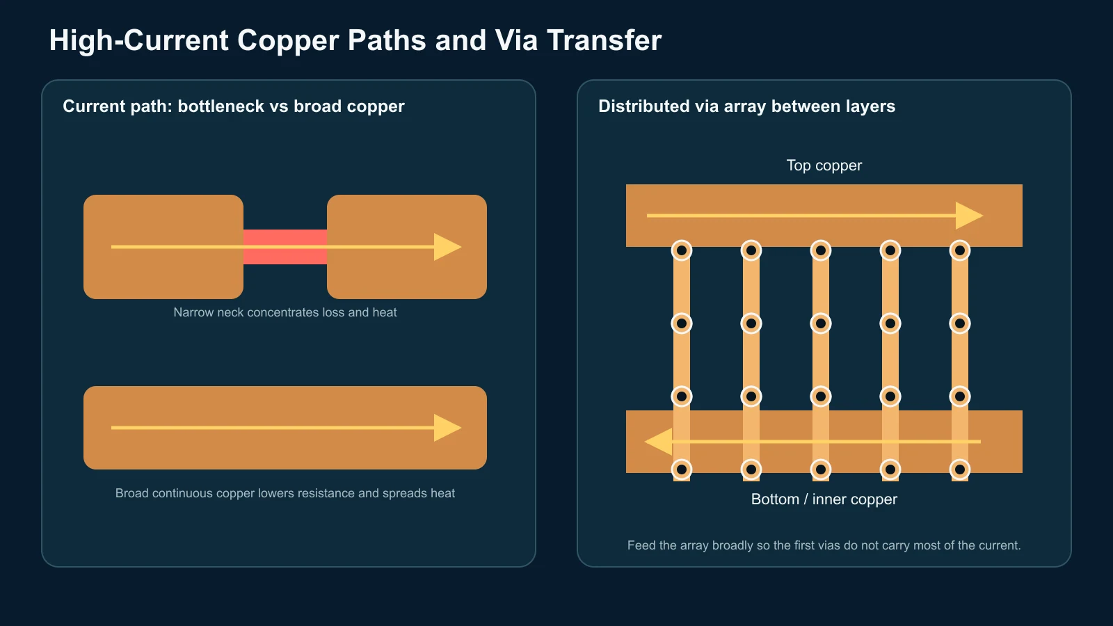
Use planes or pours where they improve resistance, inductance, and heat spreading, but inspect the actual current flow. A large copper area fed through a narrow neck is still a bottleneck. Avoid acute constrictions around pads, cutouts, mounting holes, thermal reliefs, and keepouts. For very low resistance paths, consider parallel layers, copper bus structures, embedded copper, or mechanical conductors when ordinary PCB copper is not sufficient.
5. Control parallel-layer current sharing
Parallel copper layers do not necessarily share current equally. Via placement, path length, plane geometry, temperature, and connection location determine distribution. Connect layers with distributed via arrays near current entry, exit, and transition regions. Analyze current density where one layer necks down or where vias cluster on only one side of a pad.
6. Design via arrays as current transitions
Via current capacity depends on finished hole, plating thickness, barrel length, copper connection, temperature rise, reliability, and manufacturer process. Multiple vias improve resistance and inductance only when current can spread into them effectively. Avoid a layout where the first few vias carry most of the current because the plane feeds the array from one edge. Specify plating and construction assumptions and verify them with the fabricator.
7. Separate power and sensing paths
Use Kelvin connections for shunts, current-sense resistors, regulators, and remote-sense nodes where measurement error from shared copper matters. Route sense lines away from switching nodes and connect them at the intended measurement points. Do not allow gate-drive or control returns to share noisy high-current paths unless the device application requires and accounts for it.
8. Engineer return paths and grounding
Every outgoing current has a return path. Keep the power return close enough to control loop inductance while separating noisy switching returns from sensitive analog references. Ground-plane splits can create unexpected coupling and return detours. Define where power ground, signal ground, chassis, and protective earth connect based on circuit behavior and safety requirements, not by labels alone.
9. Spread and remove heat
Use copper spreading, thermal vias, heat sinks, metal interfaces, airflow, or chassis conduction according to the thermal path. Thermal vias are effective only when they connect the hot region to copper or a structure that can absorb and remove heat. Via diameter, fill, tenting, paste behavior, and destination-plane area affect performance. Avoid placing temperature-sensitive components in the thermal wake of power devices.
10. Integrate creepage and clearance early
Reserve insulation distances before broad copper pours and heatsinks consume the board. Review spacing in three dimensions, including component bodies, exposed copper, slots, board edges, conductive hardware, and heat sinks. Heavy copper and etch compensation can change achievable spacing. If slots or coatings are used to satisfy safety objectives, document the applicable process and inspection requirements.
11. Review interfaces and protection devices
Connectors, terminals, fuses, relays, shunts, and component pads often create greater resistance than the broad traces between them. Review contact rating, terminal temperature, pad geometry, solder volume, mechanical support, and current distribution. Provide sufficient copper without creating assembly heat-sinking that prevents reliable soldering.
12. Validate electrical and thermal performance
Use DC current-density and voltage-drop analysis to identify bottlenecks. Use transient or electromagnetic analysis where switching-loop inductance, overshoot, or coupling drives risk. Verify prototypes at representative ambient, enclosure, cooling, load, and duty cycle. Measure voltage at defined points and use thermal imaging or sensors with an emissivity and access plan appropriate to the assembly.
Common Mistakes
- Choosing trace width from a current table without including length, copper, duty cycle, and cooling.
- Creating large pours connected through narrow pads, thermal reliefs, or neck-downs.
- Assuming parallel layers or all vias in an array share current equally.
- Routing the high-di/dt switching loop around convenient component placement.
- Using shared high-current copper for sensitive feedback or current measurement.
- Expanding noisy switch-node copper unnecessarily to improve apparent current capacity.
- Adding thermal vias without a useful heat destination.
- Applying generic creepage, clearance, or heavy-copper rules without the product standard and supplier process.
- Ignoring connector, fuse, shunt, and solder-joint temperature.
Manufacturing Considerations
Heavy copper PCB fabrication changes etching, undercut, minimum spacing, pad geometry, solder-mask coverage, lamination, copper balance, and finished thickness. Mixed-copper constructions can complicate impedance and resin filling. Confirm finished copper, plating, etch compensation, spacing, via structure, press construction, and allowable copper distribution through a PCB manufacturing review before design rules are locked.
Large copper areas and power components also affect assembly. Copper can pull heat from pads during reflow or hand soldering, while large components may require mechanical support and controlled paste volume. Coordinate thermal relief usage with electrical loss rather than applying one rule everywhere. Define inspection for high-current solder joints, filled vias, press-fit or bolted terminals, and any embedded or added copper structures.
Engineering Checklist
- RMS, peak, transient, startup, and fault currents documented.
- Voltage-drop and temperature limits allocated across the complete path.
- Outgoing and return-current loops mapped for each operating state.
- Power-device placement minimizes critical switching loops.
- Trace, pour, and plane geometry uses finished copper and real cooling assumptions.
- Pad necks, thermal reliefs, connectors, fuses, shunts, and vias checked for bottlenecks.
- Parallel-layer and via-array current sharing reviewed.
- Sense and feedback routes use appropriate Kelvin and quiet-return connections.
- Heat-spreading and removal paths are continuous to the environment.
- Creepage and clearance follow the applicable voltage, environment, altitude, material, and safety standard.
- Heavy-copper and assembly constraints are manufacturer-approved.
- Prototype validation covers representative load, duty cycle, ambient, and enclosure conditions.
FAQ
How wide should a high-current PCB trace be?
There is no universal width. Determine it from current waveform, trace length, finished copper, allowable voltage drop and temperature rise, layer position, neighboring copper, airflow, enclosure, ambient temperature, and manufacturer capability.
Can several PCB vias safely carry high current?
They can when the finished plating, geometry, temperature, reliability target, and current spreading support the requirement. Do not multiply a generic single-via rating by the via count without evaluating how current enters and leaves the array.
Is heavy copper always required for power electronics?
No. Wider pours, parallel layers, short paths, bus structures, thermal management, or a different architecture may meet the requirement. Heavy copper is appropriate when its electrical and thermal benefit justifies the fabrication, spacing, assembly, and cost effects.
Should thermal reliefs be removed from high-current pads?
Not as a universal rule. Solid connections reduce electrical and thermal resistance but can make soldering difficult. Select the connection style with current, loss, heat flow, component termination, soldering process, and rework requirements in mind.
Working on a High-Current or Power Electronics PCB?
Review current paths, switching loops, copper construction, via transfer, thermal management and safety spacing before release.