
Request a Design ReviewUpload Files
Email UsGet a Quote

RF PCB Design

High-frequency PCB engineering for controlled-impedance design, low insertion loss and predictable signal behavior—from stackup planning and RF layout through DFM review and prototype validation.

RF layouts built around frequency, materials and real fabrication limits

RF PCB layout guidance must account for far more than routing a trace to a nominal impedance. The laminate system, copper profile, dielectric thickness, reference planes, connector launches, component footprints and enclosure geometry all influence the final electrical behavior.

Our design workflow brings those constraints together early. We define practical transmission-line structures, protect return-current paths, manage coupling between RF, digital and power regions, and keep the layout compatible with the selected fabricator’s process capability.

Design priorities we review

Our RF PCB Design Capabilities

From architecture and stackup definition to detailed routing and release data, every stage is reviewed for RF performance, manufacturability and repeatability.

High-Frequency Routing

Precision routing for RF traces with strict impedance control

Impedance Control Design

50Ω single-ended, 90Ω differential pairs with tight tolerance.

Stack-up Engineering

Dielectric material selection (e.g., Rogers, Isola, etc.) for layer stack-up optimization.

EMI/EMC Optimization

Grounding strategy, shielding, wiring, impedance matching, and isolation techniques.

SI / PI Simulation Support

Signal integrity and power integrity analysis for validation.

Manufacturing Optimization

Design aligned with real fabrication constraints (DFM/DFT ready).

RF PCB Applications

5G Communication Modules

RF Transceivers & Front-End Modules

Radar Systems (Automotive / Defense)

Satellite Communication Systems

IoT Wireless Devices (WiFi / Bluetooth / LoRa)

Medical RF Equipment

Aerospace Electronics

RF PCB DESIGN CASE STUDIES

Representative RF projects engineered for signal integrity and production

Each RF layout begins with operating frequency, impedance targets, insertion-loss limits and enclosure constraints—then develops the stackup, transmission-line geometry, grounding and validation plan around those requirements.

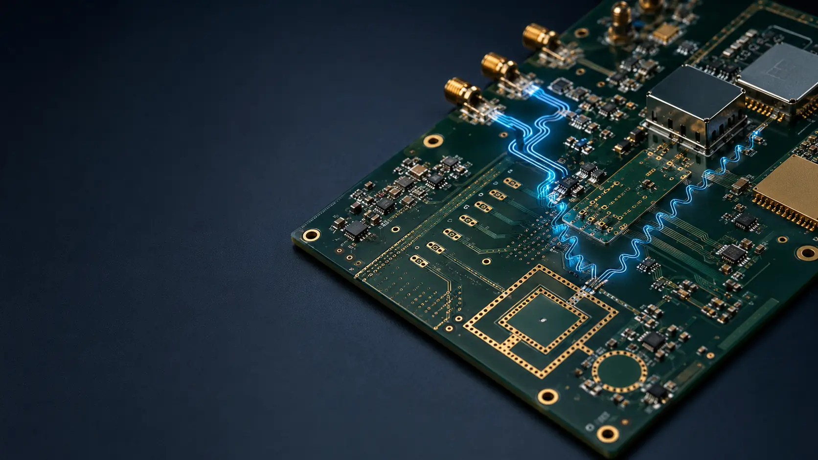
High-frequency RF PCB with controlled impedance transmission lines, microstrip structures and RF components

RF & IoT Board Engineering Scenario

An RF and IoT board project combining controlled-impedance signal paths, filtering and sensitive active devices within a restricted mechanical outline.

Design challenge
Reduce discontinuities and coupling while preserving short, predictable RF paths between the transceiver, filters and antenna interface.

Engineering approach
50Ω transmission-line control, grounded coplanar routing, via-fence planning, RF/DC zoning and component-transition optimization.

50Ω ControlGCPWVia Fencing
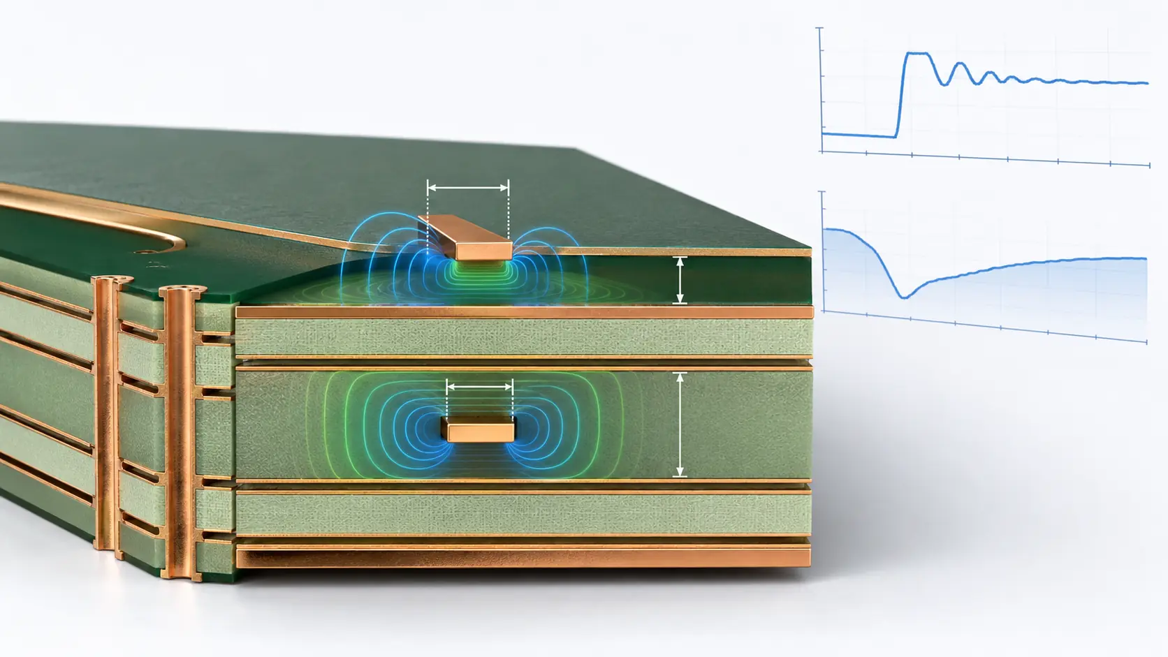
Controlled impedance PCB cross section showing microstrip, stripline, dielectric layers, ground planes, and signal integrity analysis

Microwave Control & Sensor Board

A mixed-signal microwave controller requiring stable RF performance alongside digital control, clock and power-management circuitry.

Design challenge
Prevent digital return currents and switching noise from degrading low-level RF paths across multiple functional zones.

Engineering approach
Low-loss laminate selection, microstrip/stripline transition control, return-path continuity, isolation zoning and stackup review.

Low-Loss StackupIsolationReturn Paths
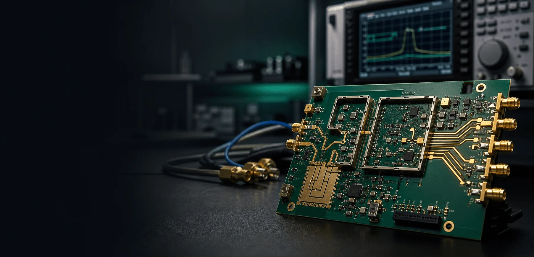
High frequency RF PCB testing setup with controlled impedance traces, SMA connectors, and microwave circuit design for advanced electronics applications.

High-Frequency Prototype Validation

An RF prototype prepared for repeatable bench evaluation, connector launch tuning and correlation between design assumptions and measured behavior.

Design challenge
Create measurement access without introducing unnecessary stubs, launch discontinuities or unstable grounding at the test interface.

Engineering approach
SMA launch optimization, calibration-aware test points, controlled reference planes and review of S-parameter and impedance results.

SMA LaunchS-ParametersValidation

These examples illustrate representative project types and engineering approaches. Details are adapted to protect customer confidentiality.

Need RF PCB Design Support?

Send us your requirements or schematics. Our RF engineers will review your project and provide optimization suggestions.

Purchasing FAQ

RF PCB Design Frequently Asked Questions

Practical answers about files, schedule, engineering support, production coordination and confidentiality.

What files do you need for RF PCB Design?

To start RF PCB Design, send your system requirements, block diagram, schematic or netlist if available, component datasheets, mechanical constraints, connector locations, stackup preferences, and any impedance, power, thermal, EMC or test requirements. Existing Gerber or ODB++ files can also help us understand a previous revision.

What is the typical lead time for RF PCB Design?

Lead time depends on design maturity, complexity, quantity, material or component availability, testing scope, and how quickly engineering questions are resolved. We confirm the schedule after reviewing your files; urgent prototype or quick-turn options can be discussed where the required process and materials permit.

Which EDA tools and file formats are supported?

We can review common production outputs such as Gerber and ODB++, as well as native EDA data when agreed during the file review. Because library versions, third-party models and tool releases vary, tell us the software and version used before transfer so we can confirm the working format or recommend a neutral export.

Can you handle an existing design or previous revision?

Yes. We can work from an existing design, production package or previous revision. We first check completeness, revision control and the requested scope, then identify any missing data, manufacturability risks or changes that need your approval before work begins.

Do you provide signal integrity and power integrity analysis?

Yes. SI/PI review or simulation can be included when the design contains high-speed interfaces, sensitive analog sections or demanding power rails. Scope depends on available stackup data, IBIS/SPICE models and measurable acceptance targets, so it is quoted separately when needed.

Can you coordinate fabrication and assembly?

Yes. Excel Circuit can coordinate engineering review, PCB fabrication, component sourcing, assembly, inspection and testing under one project. You may also order only the engineering stage and release the approved production package to another manufacturer.

How is design confidentiality protected?

Project files are limited to personnel and qualified partners who need them for quotation and delivery. Excel Circuit uses reasonable technical and organizational safeguards, does not publish customer designs without permission, and can work under a mutually agreed NDA. Your signed NDA or project agreement controls where it provides specific protections.

Final scope, price and lead time are confirmed after engineering review of your current files and requirements.