Contents
Introduction
A PCB trace is not 50 ohms because it uses a familiar width from a calculator or a previous board. It is 50 ohms only when its finished transmission-line structure—trace geometry, dielectric, copper, reference conductor, nearby copper, solder mask, and manufacturing result—produces the intended characteristic impedance over the frequency range that matters.
For hardware developed through RF PCB design or high-speed PCB layout engineering, the impedance target must also survive launches, connectors, vias, bends, pads, component footprints, layer changes, and fabrication tolerances. The correct geometry therefore comes from the actual project PCB stack-up and an agreed PCB manufacturing process. This guide explains how engineers should design and release a 50-ohm RF route without relying on a universal trace width.
Engineering Summary
- Choose the transmission-line structure and reference plane before calculating width.
- Use the fabricator’s finished stack-up, material data, copper construction, and process tolerances.
- Treat launches, vias, pads, gaps, bends, and ground stitching as part of the RF interconnect.
- Control the current return path continuously from source to load.
- Define impedance tolerance, coupon strategy, and verification method with the manufacturer.
Key Design Factors
Why 50 ohms is commonly used
Fifty ohms is widely used because many RF sources, loads, connectors, cables, instruments, and test fixtures are designed around that system impedance. It also represents a practical compromise between power handling and loss for common coaxial structures. This convention does not mean every RF network must be 50 ohms; matching networks and device ports may use other impedances internally. The PCB route should follow the interface specification and the intended reference plane.
Transmission-line structure
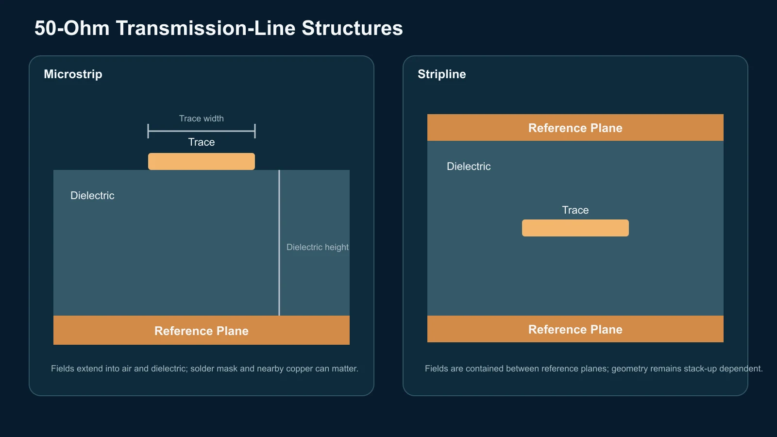
Microstrip places the route on an outer layer over a reference plane. Stripline embeds it between reference planes. Grounded coplanar waveguide adds nearby grounded copper beside the trace as well as a reference below. Each structure has different field confinement, loss, routing access, fabrication sensitivity, and grounding requirements. The same trace width will not produce the same impedance in each structure.
A broader RF layout and material strategy should be established alongside the individual 50-ohm geometry.
Material and finished geometry
Dielectric height, design Dk, copper thickness, etched trace shape, surface roughness, solder mask, and nearby copper all influence impedance. Material Dk varies with resin content, glass style, frequency, test method, and process. Use design values appropriate to the laminate construction and solver rather than copying a catalog headline number.
Detailed Engineering Guidelines
1. Define the electrical requirement
Record the nominal impedance, allowed tolerance, operating frequency range, insertion-loss budget, power level, connector interface, and verification requirement. The tolerance should reflect system margin and achievable fabrication control. Do not specify a tighter tolerance by habit; tighter limits may constrain materials, geometry, yield, and cost.
2. Select the layer and reference structure
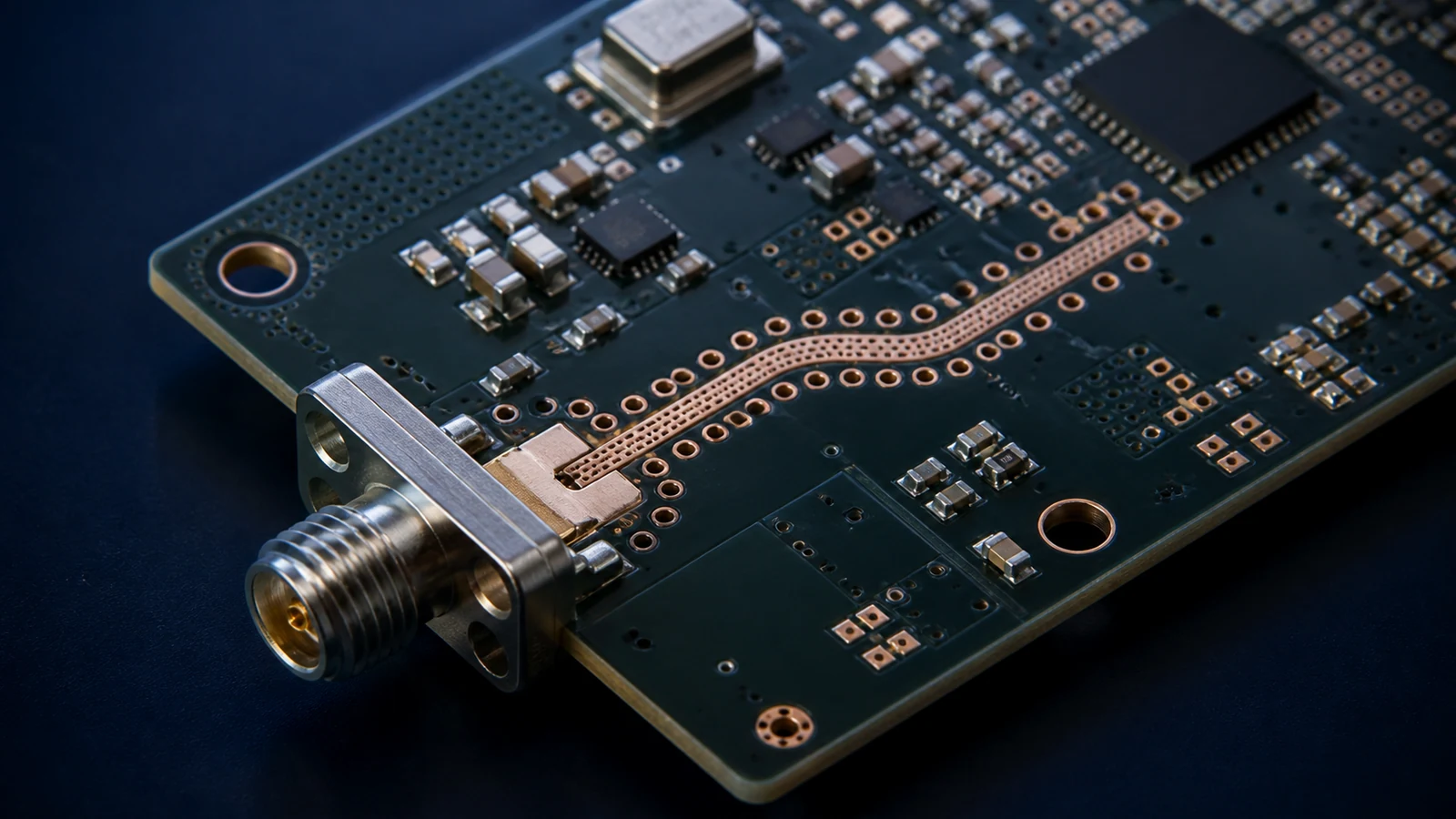
Choose an RF layer with a continuous reference plane and a practical dielectric height. Microstrip can simplify component and connector access but exposes fields to solder mask, air, and nearby structures. Stripline improves shielding but adds via transitions to surface-mounted parts. Grounded coplanar waveguide can improve isolation and field control when its side-ground spacing and via fence are designed as part of the impedance structure.
3. Calculate from the real stack-up
Use a field solver or a manufacturer-controlled impedance model with the intended dielectric thickness, material properties, finished copper, trace thickness, conductor shape, and solder mask. The required width is project-specific. It changes when prepreg thickness, resin content, copper weight, plating, or neighboring ground spacing changes. Ask the fabricator whether the supplied dimension represents base copper, finished copper, or the finished etched geometry.
4. Control the ground reference
The return current should see a continuous, low-inductance reference under or around the route. Do not cross plane splits, voids, power-island boundaries, connector cutouts, or dense antipad fields without evaluating the return path. A trace can have the correct local width and still perform poorly because its reference current must detour.
5. Design grounded coplanar structures as a system
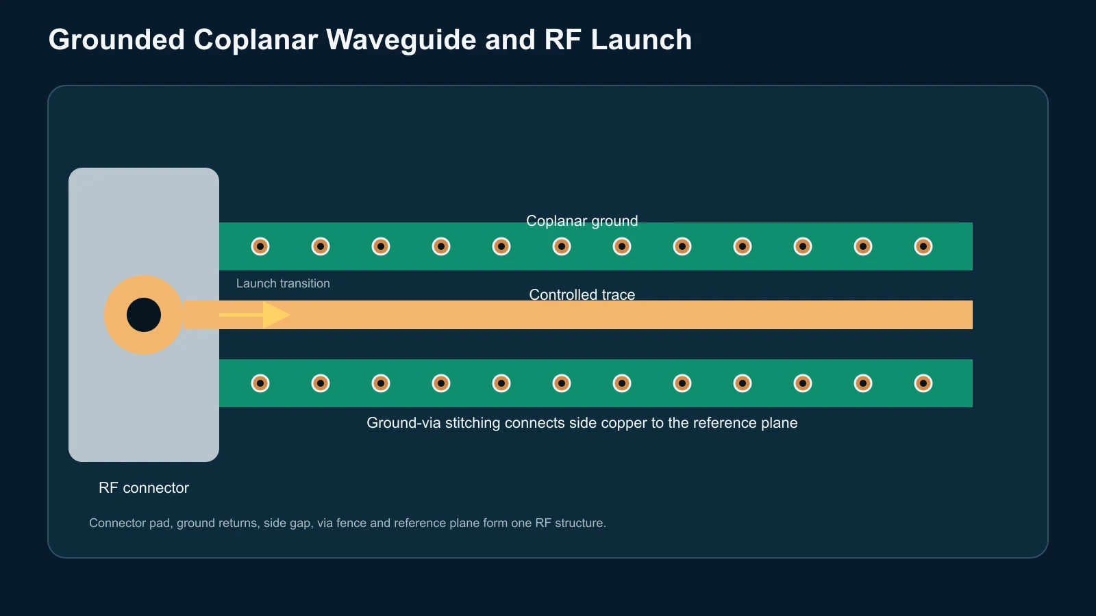
For grounded coplanar waveguide, trace width, side gap, dielectric height, copper thickness, and reference connection all influence impedance. Side ground that is too far away may have little effect; ground that moves closer without recalculation changes the impedance. Use stitching vias to connect side copper to the reference plane, but determine spacing from the frequency range, field containment, geometry, and manufacturing capability rather than applying a universal pitch.
6. Treat connectors and launches as transitions
An RF connector launch includes the connector pin, pad, anti-pad, ground pads or ground posts, reference plane opening, and the transition into the controlled line. Optimize the launch for the selected connector and board thickness. Vendor reference layouts are useful starting points, but they must be adapted to the actual stack-up. Avoid large pads or abrupt neck-downs that create excess capacitance or inductance.
The transition approach used in an RF and IoT board case study can help frame launch, grounding, and production-review decisions.
7. Engineer layer transitions
A signal via introduces barrel inductance, pad capacitance, anti-pad geometry, and potentially a stub. Place ground-return vias near the transition so the return current can change layers with the signal. Through-via stubs may require back drilling, blind vias, or a different layer assignment when their resonance or added loss threatens the channel budget. The correct choice depends on board thickness, frequency, via geometry, and fabrication capability.
8. Minimize impedance discontinuities
Keep line geometry consistent through bends, component pads, test features, and routing obstacles. Curved or mitered bends may be useful where geometry would otherwise create excess capacitance, but the need depends on frequency and line dimensions. Avoid unnecessary test pads, long component pad transitions, reference voids, and sudden changes in adjacent copper. Model electrically long or geometrically severe transitions.
9. Manage coupling and isolation
Spacing from other RF routes, digital clocks, power-switching nodes, board edges, shields, and grounded metal affects coupling and impedance. There is no universal spacing multiple that solves every case. Base separation on field structure, frequency, parallel length, isolation target, shielding, and stack-up. Preserve the intended coplanar gap around the route; copper-pour cleanup can unintentionally alter it.
10. Coordinate manufacturing and verification
Release the impedance requirement by layer, structure, target, and tolerance. Identify whether solder mask is included, specify the reference plane, and provide an impedance table linked to the approved stack-up. Agree on whether the fabricator may adjust trace width or dielectric selection, how changes will be approved, and whether TDR coupons or additional RF test structures are required.
Common Mistakes
- Using a trace width copied from another PCB with a different stack-up.
- Entering a generic FR-4 Dk without matching laminate construction or solver method.
- Ignoring plating, etched sidewall shape, solder mask, or copper roughness.
- Routing across reference-plane gaps while maintaining nominal trace width.
- Adding coplanar ground after impedance calculation without recalculating the structure.
- Using sparse or poorly connected ground vias around a coplanar route or transition.
- Treating the connector pad and signal via as electrically transparent.
- Specifying 50 ohms on the drawing without defining layer, reference, tolerance, or test method.
Manufacturing Considerations
Impedance depends on the finished board, not only CAD dimensions. Etch compensation, copper plating, press thickness, resin flow, glass style, trace location relative to weave, solder mask thickness, and material lot behavior affect the result. Work with the selected manufacturer before layout sign-off and use the approved stack-up in the PCB rules.
A TDR coupon can demonstrate the coupon structure produced on the panel, but it does not prove that every transition, connector launch, or reference discontinuity on the product board is correct. Define coupon geometry that represents the production layer and construction. For demanding RF channels, combine fabrication control with SI / PI analysis, launch validation, or appropriate insertion-loss and return-loss measurements.
Engineering Checklist
- Interface impedance, tolerance, frequency range, and loss budget documented.
- Microstrip, stripline, or coplanar structure intentionally selected.
- Approved material and finished stack-up used for calculation.
- Dk, dielectric height, copper thickness, trace shape, and solder mask accounted for.
- Reference plane is continuous along the complete route.
- Coplanar gap and ground-via strategy included in the impedance design.
- Connector launches, component pads, bends, and test features reviewed.
- Signal-via transitions include nearby return paths and acceptable stub behavior.
- Manufacturer adjustment and approval rules documented.
- Coupon and validation method match the project risk.
FAQ
What PCB trace width gives exactly 50 ohms?
There is no universal width. It depends on the transmission-line structure, dielectric height and Dk, finished copper, trace shape, solder mask, adjacent ground, and manufacturing process. Calculate it from the approved project stack-up.
Is a 50-ohm microstrip the same width as a 50-ohm stripline?
No. Their field structures and reference geometry differ. Even two microstrip layers can require different widths when dielectric height, copper, or material construction changes.
Does a ground pour beside an RF trace guarantee coplanar waveguide behavior?
No. The side-ground gap, connection to the reference plane, via stitching, dielectric height, and trace width must be designed together. Uncontrolled nearby copper may simply change impedance or create resonant structures.
Does passing a 50-ohm TDR coupon validate the complete RF path?
It validates the representative coupon within the measurement method and tolerance. It does not independently validate connectors, vias, pads, bends, or plane discontinuities on the product board.
Working on an RF PCB?
Align the transmission-line structure, connector launch, return path and manufacturing tolerance before releasing RF geometry.