Contents
A PCB manufacturing production package is the controlled set of fabrication, assembly, component and test data that a supplier uses to build and verify a printed circuit board assembly. For a bare PCB, the package normally includes Gerber or ODB++ data, NC drill files, a fabrication drawing and a readme. For an assembled board, add a bill of materials (BOM), centroid or pick-and-place data, assembly drawings and test requirements. Every file must identify the same board revision.
This checklist explains which PCB manufacturing files are required, what each file controls, how to prevent revision conflicts and what Excel Circuit engineers review before releasing a design to fabrication or turnkey PCBA production.
What files are required for PCB manufacturing?
A production-ready bare-board package requires image data for every manufactured layer, drill data for every hole type, mechanical definitions for the finished board and written requirements that cannot be encoded safely in layer artwork.
| File or document | Bare PCB | PCBA | What it controls |
|---|---|---|---|
| Gerber X2, RS-274X or ODB++ | Required | Required | Copper, solder mask, silkscreen, paste and board outline layers |
| NC drill files | Required | Required | Plated and non-plated holes, slots and tooling holes |
| Fabrication drawing | Required | Required | Dimensions, stackup, materials, tolerances, finish and special notes |
| Netlist | Recommended | Recommended | Independent electrical connectivity reference |
| BOM | Not applicable | Required | Approved component identities, quantities and sourcing instructions |
| Centroid / pick-and-place file | Not applicable | Required for SMT | Component coordinates, rotation and board side |
| Assembly drawings | Not applicable | Required | Reference designators, polarity, fitted status and process notes |
| Test specification | As required | As required | Electrical test, programming, ICT or functional acceptance criteria |
| Readme and revision record | Required | Required | Package identity, revision, exceptions and precedence rules |
The exact deliverable set depends on whether the supplier will fabricate a bare board, assemble consigned components or manage a complete turnkey build. That scope must be stated before the supplier reviews the files.
1. Gerber or intelligent PCB fabrication data
Gerber and ODB++ files define the two-dimensional artwork used to manufacture each PCB layer. A complete Gerber package includes every copper layer, top and bottom solder mask, top and bottom silkscreen, paste layers when required and one unambiguous board outline.
- Export all layers from one approved PCB database and one revision.
- Use clear file names that identify the layer function rather than relying only on software-specific extensions.
- Confirm that positive and negative planes render correctly.
- Include rout, cutout and scoring information without duplicating conflicting outlines.
- View the exported dataset in an independent CAM viewer before release.
Our Gerber file checklist for PCB manufacturing provides a layer-by-layer review, while the Altium Gerber export guide explains the export settings. If ODB++ or IPC-2581 is supplied, identify it as the controlling dataset and do not include an older Gerber set unless the readme explains which source takes precedence.
2. NC drill files and hole definitions
NC drill files define hole coordinates and tool diameters for plated through holes, non-plated holes, vias and slots. Separate plated and non-plated data whenever the CAD export supports that distinction, and state whether each diameter represents the drilled size or finished hole size.
The drill dataset must use the same origin, units and zero-suppression convention as the image data. The fabrication drawing should identify finished hole tolerances, press-fit holes, countersinks, counterbores, castellations, controlled-depth drilling and any slot that cannot be interpreted reliably from a standard drill hit.
3. PCB fabrication drawing
A PCB fabrication drawing is the authoritative mechanical and process specification for the finished bare board. It should resolve requirements that are missing or ambiguous in the artwork.
- Finished board dimensions and dimensional tolerances
- Board thickness and thickness tolerance
- Layer count and approved stackup
- Base material, minimum Tg and other required laminate properties
- Finished copper weight or copper thickness by layer
- Controlled-impedance targets, tolerance and coupon requirements
- Surface finish and any selective finish
- Solder mask color and silkscreen color
- Minimum finished hole size and special hole requirements
- Edge plating, bevels, castellations, scoring and routing notes
- Applicable IPC class, acceptance criteria and electrical-test requirement
The drawing and artwork must agree. When a note specifies a six-layer board but the data contains eight copper layers, production should stop until the discrepancy is resolved. A structured PCB design for manufacturability review catches these conflicts before material is released.
4. Stackup and controlled-impedance requirements
The PCB stackup defines the order, thickness and material system of copper, core and prepreg layers. For controlled-impedance designs, it must also identify the target impedance, signal layer, reference plane, trace type and permitted tolerance.
Do not lock every dielectric thickness unless the construction has already been approved with the intended manufacturer. Fabricators may need to adjust dielectric thickness or trace geometry to match available laminates and press conditions. Define the electrical target and critical material properties, then document who may approve the final production stackup. See our PCB stackup design guide for layer-planning and impedance considerations.
5. Netlist and electrical-test data
An IPC-D-356 netlist provides an independent description of PCB connectivity for CAM comparison and bare-board electrical test. It helps detect artwork errors, missing connections and unintended shorts that visual layer inspection may not reveal.
Specify whether flying-probe or fixture-based electrical testing is required and define any exceptions, such as isolated copper, intentional opens or components embedded in the bare-board structure. The electrical-test requirement belongs in the fabrication notes even when the netlist is included.
What additional files are required for PCB assembly?
PCB assembly requires component identity, placement, orientation and acceptance data in addition to the bare-board fabrication package. The BOM, centroid file and assembly drawing must use the same reference designators.
Bill of materials
The BOM controls which components may be purchased and fitted. Each populated line should include reference designators, quantity per board, manufacturer, manufacturer part number, value or description, package and sourcing status. Mark do-not-fit items explicitly rather than deleting them from only one file.
Use the PCB assembly BOM guide to prepare manufacturer part numbers, approved alternatives and DNP conventions. A turnkey supplier also needs substitution authority: no substitutions, approved vendor list only, or engineering approval required.
Centroid or pick-and-place data
A centroid file defines each machine-placed component by reference designator, X coordinate, Y coordinate, rotation and board side. Its coordinate origin must match the assembly drawing or be explained in the readme.
Rotation conventions vary between CAD libraries and assembly equipment. The supplier should compare several polarized and asymmetric packages against the drawing before programming the placement machine. Our SMT pick-and-place file format guide lists the required columns and validation checks.
Assembly drawings and special instructions
Assembly drawings show component location, reference designators, polarity and the fitted status of each side. Add separate instructions for press-fit connectors, hand-soldered parts, adhesive, staking, conformal coating, thermal compounds, depanelization restrictions and customer-supplied components.
Programming and test requirements
Programming and test files define how the assembled board will be verified and what constitutes a passing unit. Supply released firmware, programming instructions, checksum or version identity, connector pinouts, fixture information, power limits and measurable acceptance criteria.
- AOI: define workmanship standard and any areas that require manual inspection.
- X-ray: identify hidden-joint packages such as BGA, LGA, QFN or bottom-terminated power devices.
- ICT or flying probe: provide test-point access and a netlist-compatible fixture dataset.
- Functional test: provide power-up sequence, loads, stimuli, expected outputs and pass/fail limits.
- Firmware programming: identify the released binary, target device, interface, security settings and verification method.
Test coverage should match product risk and production volume. Excel Circuit can align inspection and test planning with the project through its PCB testing services.
How should revisions and file names be controlled?
Revision control requires every production document to identify one consistent board revision and release state. A supplier should never have to infer whether “final,” “final2” or an email attachment is authoritative.
- Assign a unique project or part number and PCB revision.
- Export every manufacturing file from the approved design database.
- Place the files in one release folder with a clear revision and date.
- Include a readme that lists the controlling files and approved exceptions.
- Remove obsolete, duplicate and intermediate outputs.
- Generate a checksum or retain a controlled archive for later comparison.
- Require written approval for any supplier-proposed data change.
If fabrication and assembly use different part numbers or revisions, provide a mapping table. Panel drawings should identify both the array revision and the individual PCB revision.
Pre-release PCB manufacturing file checklist
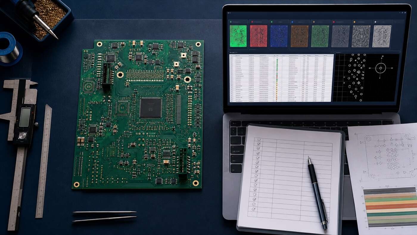
A pre-production DFM/DFA review confirms that the package is complete, internally consistent and suitable for the intended manufacturing scope.
- All copper, mask, legend and mechanical layers are present.
- The board outline is closed, unique and dimensionally correct.
- Drill coordinates align with copper and mechanical data.
- Plated, non-plated and slotted holes are identified.
- Layer count, stackup, material and finished thickness agree.
- Surface finish, copper weight and solder mask requirements are stated.
- Impedance requirements identify nets, layers, targets and tolerances.
- The BOM, centroid data and assembly drawings share identical designators.
- DNP components are marked consistently in every assembly file.
- Component polarity and pin-1 orientation have been checked.
- Firmware and test instructions identify released versions and pass limits.
- Every file belongs to the same approved revision.
- The archive opens correctly and contains no passwords or corrupted files.
Common production-package errors
The most damaging production-package errors are conflicts between otherwise valid files. Typical examples include an outdated BOM paired with a new placement file, a drawing that specifies a different finish from the purchase order, mirrored bottom-side coordinates, duplicate board outlines and drill files exported in the wrong units.
Do not correct these discrepancies through informal assumptions. Record each issue in an engineering query, identify the affected revision and obtain an approved answer before production continues. This creates traceable verification evidence and prevents the same ambiguity from returning during a repeat order.
Submit a production-ready PCB package
Excel Circuit provides custom electronics production support across PCB design, fabrication, component sourcing, in-house SMT assembly and turnkey PCBA from prototype through production. Send the available Gerber or ODB++ data, NC drill files, fabrication drawing, BOM, pick-and-place file and test requirements for an engineering review. These deliverables become inputs to the complete PCB manufacturing process.
Frequently asked questions
Can a PCB manufacturer build a board from Gerber files only?
A manufacturer can sometimes quote a simple bare PCB from Gerber and drill files, but production still requires confirmed dimensions, thickness, material, copper weight, surface finish and other fabrication requirements. A fabrication drawing and readme remove ambiguity.
Is a BOM required for bare PCB manufacturing?
No. A BOM identifies electronic components and is required for PCB assembly, not for ordinary bare-board fabrication. The bare-board material and construction requirements belong in the fabrication drawing and stackup.
What is the difference between a centroid file and an assembly drawing?
A centroid file gives machine-readable component coordinates, rotation and board side. An assembly drawing gives a human-readable visual reference for location, designator, polarity and special assembly instructions. Reliable assembly uses both.
Should source PCB design files be included?
Source CAD files are useful when the supplier will perform engineering changes, DFM correction or design support. If the supplier is building an approved design without modification, released manufacturing outputs remain the controlling production data unless the purchase agreement states otherwise.