Contents
How Much Does PCB Layout Cost?
PCB layout is normally quoted from engineering scope and complexity rather than one public fixed price. The workload depends on schematic size, component and pin count, package density, BGA escape, layer and stackup needs, high-speed or RF constraints, HDI structures, SI/PI scope, mechanical restrictions, DFM/DFA, deliverables, schedule, and expected revisions. Two boards with the same component or pin count can therefore require very different layout effort.
This page explains the cost model and the information needed for an accurate quotation. It does not publish an Excel Circuit price list, convert schedule into price, or present competitor rates as company pricing.
What Determines PCB Layout Service Cost?
PCB layout service cost is determined by the PCB layout engineering workflow required to define, implement, review, and release the board. Estimators consider design size, package and routing density, electrical constraints, analysis responsibilities, mechanical limits, manufacturing rules, deliverables, review cycles, and the maturity of customer inputs. A quotation is more reliable when those responsibilities and assumptions are explicit before work begins.
| Cost driver | Why it changes engineering effort | Example |
|---|---|---|
| Design size | More components, pins, nets, and schematic pages increase placement, routing, checking, and documentation scope | Large component population or several functional blocks |
| Fine-pitch BGA or HDI | Escape, via architecture, stackup, routing-layer allocation, and fabrication coordination become interdependent | Microvia or via-in-pad evaluation for a dense package |
| DDR and high-speed channels | Topology, impedance, timing, skew, return paths, transitions, and constraint verification require added planning | DDR, PCIe, Ethernet, USB, or SerDes implementation |
| RF, analog, or power circuitry | Grounding, coupling, materials, current paths, thermal behavior, safety spacing, and EMI may constrain placement and routing | RF connector transition, sensitive ADC reference, or switching-power loop |
| SI/PI or advanced analysis | Model preparation, simulation, review, and reporting are additional engineering activities when included | Channel review or PDN analysis |
| Mechanical constraints | Fixed connectors, outline, mounting, keepouts, height limits, and enclosure features reduce placement freedom | Dense board inside a fixed enclosure |
| DFM/DFA and manufacturing rules | Fabrication and assembly capability must be coordinated with the implemented geometry and outputs | Controlled stackup, via fill, inspection, or test-access requirements |
| Revisions and ECOs | Changes after planning or routing can require replacement, rerouting, constraint updates, and renewed checks | Connector, package, pinout, schematic, or enclosure change |
Does Pin Count Determine PCB Layout Price?
Pin count does not determine PCB layout price by itself; it is a useful indicator of project scale. More pins can mean more nets, placement decisions, routing, review, and documentation, but the count does not reveal package pitch, board density, interface constraints, analysis scope, or mechanical freedom. A lower-pin design with a fine-pitch FPGA, dense DDR, and tight enclosure can require more effort than a larger low-speed design.
“Cost per pin” is not one standardized industry method because suppliers may count physical pins, routed pins, or electrical connections differently and may include different engineering responsibilities. Before comparing a per-pin estimate, confirm the counting basis, included reviews, deliverables, revision assumptions, and exclusions.
Typical PCB Layout Lead-Time Planning by Pin Count
The ranges below are verified Excel Circuit planning guidance. They are schedule ranges, not pricing tiers, and must not be converted mathematically into a price.
| Project pin count | Typical planning range |
|---|---|
| Under 1,000 pins | 3–5 working days |
| 2,000–3,000 pins | 5–7 working days |
| 4,000–5,000 pins | 8–12 working days |
| 6,000–9,000 pins | 15–18 working days |
| 10,000–13,000 pins | 18–20 working days |
| 14,000–15,000 pins | 20–22 working days |
| 16,000–20,000 pins | 22–30 working days |
Actual schedule depends on design complexity, BGA density, interface constraints, required analysis, review scope, and completeness of project inputs. Projects between the listed planning bands require individual review.
BGA, HDI, and Stackup Cost Drivers
Why do BGA and HDI projects require more engineering effort?
BGA and HDI projects can require more engineering effort because package pitch, ball distribution, escape routing, via strategy, stackup, routing layers, power access, and fabrication capability must be coordinated. Microvias, blind or buried vias, and via-in-pad are evaluated only when the package and construction justify them. The added effort comes from interdependent planning and review, not a fixed BGA or HDI surcharge.
A design with many simple connector and low-speed pins may be easier than a smaller design dominated by a fine-pitch FPGA BGA and dense memory. The BGA Fanout Guide explains escape trade-offs, while the HDI PCB Design page describes the professional engineering context.
Does higher PCB layer count automatically mean higher layout cost?
Higher PCB layer count does not automatically mean higher layout cost because layers are part of the routing and reference architecture, not a standalone pricing multiplier. More layers can add stackup, signal-allocation, plane, via, and documentation decisions, yet they can also reduce routing congestion and improve reference continuity. The quotation depends on why the layers are needed and how they affect breakout, impedance, power distribution, and manufacturing coordination.
Trying to force a constrained design onto too few layers can increase placement iteration, routing difficulty, and review risk. Stackup should be selected from the electrical, mechanical, and fabrication requirements rather than from a price formula. For deeper layer-planning context, see the PCB Stackup Guide.
High-Speed, FPGA, RF, Power, and Analog Scope
How do high-speed requirements affect PCB design cost?
High-speed requirements can increase PCB design cost by adding stackup planning, controlled-impedance rules, topology, timing or skew constraints, return-path review, via-transition planning, crosstalk control, and verification. The effort depends on the actual channel and requested analysis, not the protocol name alone. Implementing supplied constraints is also a different scope from developing models, running SI simulation, and producing a formal report.
DDR, PCIe, high-speed Ethernet, USB, and SerDes can compete for placement and routing channels around processors or BGAs. Use the DDR Routing Guidelines for memory-specific trade-offs and High-Speed PCB Design for the service context.
FPGA and embedded boards
FPGA projects may combine high pin count, BGA breakout, DDR, transceivers, multiple rails, clocks, and SI/PI constraints, but not every FPGA board has the same complexity. Architecture, package, utilization, interfaces, board area, stackup, and manufacturing rules determine the work. The Embedded & FPGA PCB Design Guide shows how those decisions interact at system level.
RF design
RF scope may include controlled impedance, material and stackup selection, grounding, path planning, antenna or connector transitions, RF/digital isolation, and fabrication coordination. Not every RF board requires specialty laminate, and there is no universal RF premium; materials and analysis should follow the actual frequency, loss, power, environment, and interface requirements.
Power electronics
Power-board effort can be driven by current paths, copper construction, thermal management, switching loops, EMI, creepage and clearance, mechanical heat-sink constraints, and manufacturing limits. A simple connection count does not express current density, safety, thermal, or switching-loop risk, so these requirements should be visible during quotation.
Analog and mixed signal
A small analog or mixed-signal board can be engineering-intensive when it contains sensitive nodes, ADC or DAC interfaces, reference voltages, filtering, grounding, or shared analog/digital return structures. Physical size and pin count alone do not show the placement, isolation, coupling, and power-supply decisions needed to preserve performance.
Separate Layout from Optional Engineering Analysis
PCB layout normally covers placement, routing, design-rule implementation, checking, documentation, and agreed manufacturing outputs. Depending on the project, separate or additional scope may include constraint development, detailed stackup engineering, SI analysis, PI/PDN review, simulation, advanced thermal analysis, or formal reports. A quotation should say which activities are included, optional, supplied by the customer, or excluded.
Every project does not require identical SI/PI simulation. Analysis is most valuable when it resolves a defined risk or design decision. The PCB Layout Optimization article explains the engineering relationships without defining commercial scope.
Schematic and Mechanical Input Quality
Why does schematic quality affect quotation accuracy?
Schematic quality affects quotation accuracy because incomplete connectivity, unclear net names, missing packages, undefined interfaces, unassigned FPGA pins, unresolved power architecture, and changing parts create clarification and rework. A stable schematic with known constraints lets the estimator identify placement, routing, review, and deliverable scope more confidently. An early estimate is still possible from partial data, but its assumptions and open decisions should be stated.
Mechanical inputs can be equally important. A board outline, DXF or STEP model where available, connector and mounting-hole positions, keepouts, height restrictions, enclosure boundaries, antennas, shields, and heat-sink features determine placement freedom. Not every project needs every file type; provide the information that controls the physical implementation.
Fabrication, DFM, and DFA Affect Total Project Cost
Layout geometry must match the intended manufacturing capability for trace/space, stackup, controlled impedance, materials, copper weight, via construction, HDI, mask, assembly clearance, inspection, and test access. Excel Circuit can coordinate design requirements with qualified PCB manufacturing resources and in-house SMT assembly; this is not a claim of in-house PCB fabrication.
A lower layout quote is not necessarily the lower-cost project if it omits DFM/DFA or produces avoidable fabrication difficulty, unnecessary HDI, assembly problems, poor test access, or a redesign. Compare layout cost with downstream build, inspection, debug, and release risk rather than treating the PCB database as an isolated deliverable.
Revisions, ECOs, and Scope Boundaries
Quotation scope should define review gates, responsibilities, deliverables, and how changes are evaluated. Normal corrections to agreed work differ from a scope change such as a new schematic block, package substitution, connector relocation, enclosure change, FPGA pin reassignment, additional interface rule, or major placement revision. These changes may require replacement, rerouting, updated constraints, renewed DRC, documentation, and manufacturing review.
No universal revision policy is assumed here. Buyers should ask each supplier how review comments, ECOs, customer delays, and post-layout manufacturing feedback are handled.
What Files Are Needed for a PCB Layout Quote?
A PCB layout quotation is most accurate when the customer provides the available schematic, BOM or component list, board outline, mechanical and placement constraints, key interfaces, package information, stackup or impedance requirements if known, manufacturing constraints, requested deliverables, and target schedule. For FPGA work, include the package, pin assignment, memory, and transceiver information. Existing PCB source data is useful for redesign projects.
Datasheets or reference designs are helpful for unusual components and interfaces, but unnecessary confidential files should not be requested. An NDA can be arranged before detailed file review where appropriate. Partial information can support an early scope discussion when assumptions and items awaiting confirmation are clearly identified.
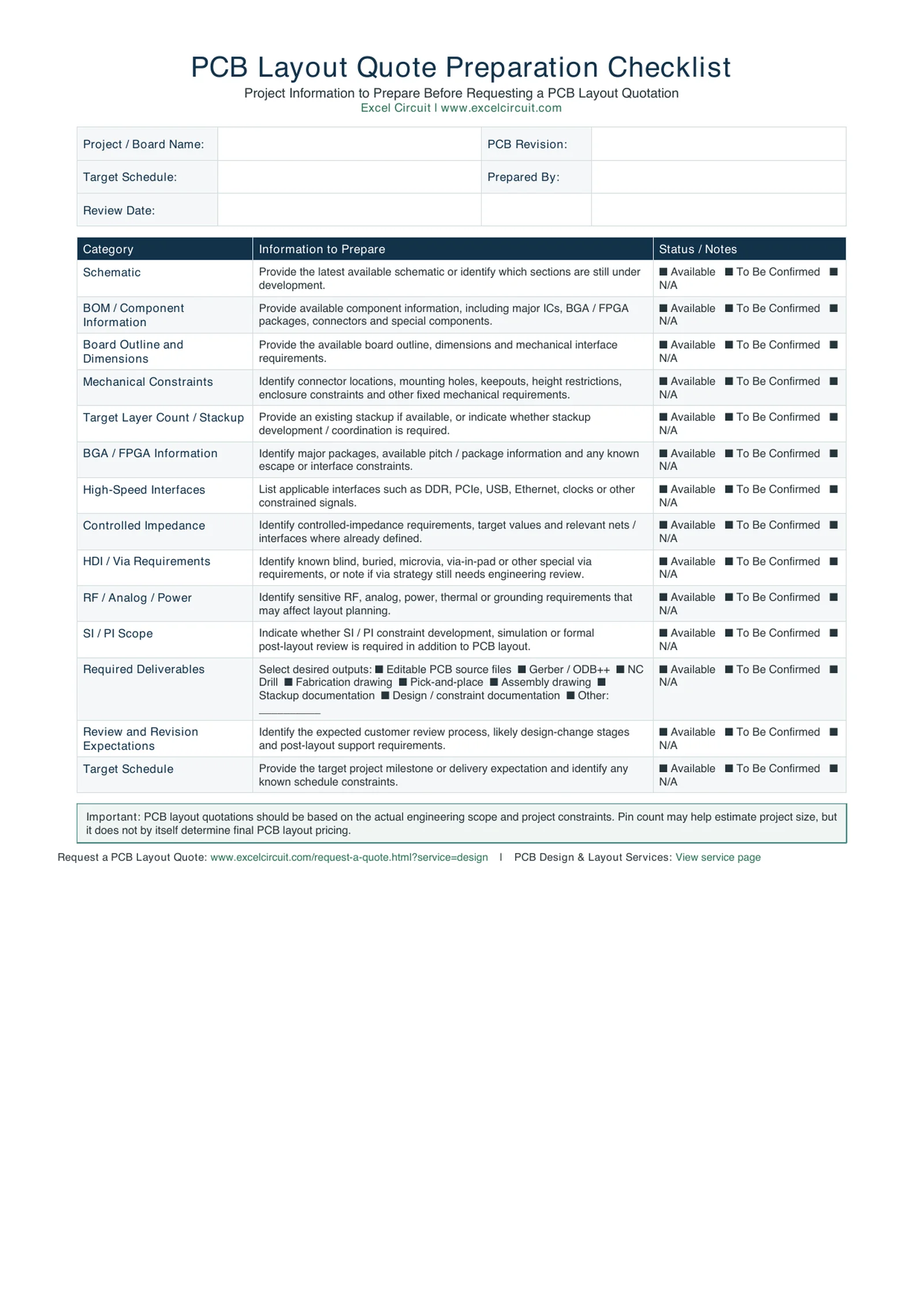
PCB Layout Quote Preparation Checklist
- Schematic and current revision status
- BOM, package information, and verified footprints or libraries where available
- Board outline, connector positions, mounting, keepouts, height, enclosure, and other mechanical constraints
- Key interfaces, clocks, RF, analog, power, and controlled-impedance requirements
- BGA or FPGA package, pin assignment, memory, transceiver, and escape information
- Target stackup, materials, via structures, or qualified fabricator constraints if known
- Requested SI/PI, thermal, DFM/DFA, documentation, and manufacturing-support scope
- Required editable source, fabrication, assembly, and review deliverables
- Expected review process, known ECOs, milestones, and target schedule
How the Quotation Workflow Works
- Confidentiality: arrange an NDA before detailed review if required.
- Project submission: send the available design, mechanical, constraint, deliverable, and schedule information.
- Engineering review: identify design size, packages, interfaces, stackup, manufacturing needs, analysis scope, assumptions, and open items.
- Effort and schedule planning: estimate the layout and agreed engineering workload using the actual constraints.
- Quotation: issue a project-specific scope, responsibilities, deliverables, schedule basis, and commercial terms.
- Scope confirmation: resolve assumptions and confirm the baseline before work starts.
This workflow does not promise instant pricing or a universal response time. Projects with incomplete inputs can begin with a preliminary scope discussion.
How Should PCB Layout Quotations Be Compared?
PCB layout quotations should be compared by aligning scope, assumptions, responsibilities, deliverables, schedule basis, and revision terms before comparing the headline figure. Check whether schematic review, stackup planning, BGA fanout, DDR and high-speed constraints, DFM/DFA, SI/PI, editable source data, manufacturing outputs, engineering communication, NDA handling, and fabrication or assembly transition support are included, optional, or excluded.
Useful comparison questions include:
- Does the quotation cover placement, routing, constraint setup, checking, and manufacturing documentation?
- Who owns stackup, impedance, BGA breakout, HDI, and fabricator coordination?
- Are SI/PI implementation, simulation, review, and reporting clearly separated?
- Which editable source files, Gerber or other manufacturing data, drawings, and records will be delivered?
- How are customer reviews, ECOs, post-layout support, and schedule dependencies handled?
- Is support for the manufacturing and assembly handoff included?
Neutral, like-for-like scope comparison is more informative than ranking suppliers only by a unit rate or total headline.
Why Can the Lowest PCB Design Quote Cost More Overall?
The lowest PCB design quote can create a higher total project cost when essential engineering, source deliverables, DFM/DFA, constraint work, or transition support is excluded. Missing scope can surface later as redesign, added board spins, assembly problems, manufacturing delay, SI/PI debug, or component and package changes. The commercial decision should consider the complete hardware-development outcome, not assume the lowest layout line item is the lowest-risk result.
Outsourcing can be useful when an internal team lacks specialist layout capacity, faces a short-term workload peak, or needs support for dense BGA, DDR, RF, or other constrained work. It is not automatically better than internal layout; compare technical ownership, communication, schedule, confidentiality, and handoff needs.
Excel Circuit Capability Context
Relevant verified capability includes PCB designs up to 42 layers, minimum trace/space support of 2.4 mil, high-frequency design support up to 60 GHz, minimum BGA pitch of 0.3 mm, and maximum BGA pin count of 2912. Supported EDA environments include Altium Designer, Cadence Allegro, Siemens PADS, and Siemens Xpedition. These metrics describe capability limits, not pricing criteria; an in-range project still requires scope review.
For professional evaluation of the required engineering scope, deliverables, and manufacturing handoff, review PCB Design & Layout Services.
Frequently Asked Questions
How much does PCB layout typically cost?
There is no verified universal Excel Circuit PCB layout price published on this page. Cost depends on the project-specific engineering scope, including schematic maturity, routing complexity, packages, stackup, interfaces, analysis, mechanical constraints, deliverables, revisions, and schedule. Pin count can support early sizing, but a commercial figure requires review of the available design files and requirements.
Is PCB layout pricing based on pin count?
Pin count can indicate project scale, but it is not a final-price formula. Suppliers may also count pins differently. Package density, BGA escape, high-speed constraints, layers, mechanics, manufacturing rules, analysis, documentation, and revisions determine the actual workload, so the project scope must be reviewed.
Why does BGA layout cost more?
A BGA can require added effort when pitch, ball distribution, escape density, via technology, stackup, power access, placement, or interface routing is constrained. The package label and ball count do not create a fixed surcharge. The implemented fanout, manufacturing coordination, and review responsibility define the work.
Does layer count affect PCB design cost?
Layer count can affect stackup, signal allocation, planes, via transitions, impedance, power distribution, and documentation, but the relationship is not linear. More layers can sometimes make routing and references clearer. Cost depends on why the layers are needed and how they interact with the design.
What files are needed for a PCB layout quote?
Provide the available schematic, BOM or component information, board outline, mechanical constraints, key interfaces, package information, manufacturing requirements, requested deliverables, and schedule. Include FPGA pin and memory/interface data when relevant. An NDA can be arranged before detailed review, and partial inputs can support a preliminary discussion.
Can I get a PCB layout quote before the schematic is fully finalized?
An early estimate may be possible from the available information if assumptions, open decisions, and exclusions are documented. Later schematic, package, mechanical, interface, or deliverable changes can alter the engineering workload, so the final scope, schedule, and commercial terms may need confirmation after the inputs stabilize.
Request a PCB Layout Quotation
To receive a PCB layout quotation, send the available schematic, board outline, BOM, key interface requirements, package or BGA information, and any stackup or manufacturing constraints. An NDA can be arranged before detailed file review.