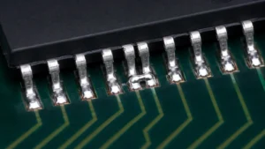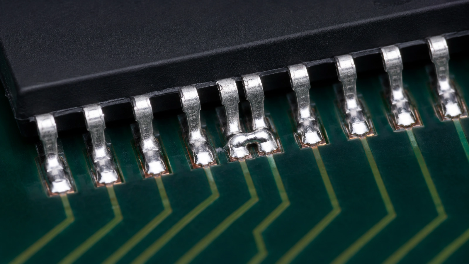
Solder bridging occurs when solder creates an unintended conductive connection between adjacent pads, component leads or joints. It can produce an electrical short and may be visible between fine-pitch leads or hidden beneath a package. Excess paste is one possible cause, but stencil geometry, print misalignment, placement, pad design, solder-mask limitations, reflow behavior and surface condition can also contribute.
Correct the cause by finding where the assembly first departed from the intended condition: printing, placement, reflow or a later operation. Removing a visible bridge repairs the immediate defect; it does not establish why the bridge formed or prevent the next one.
| Possible contributor | Possible mechanism | What to inspect | Corrective direction |
|---|---|---|---|
| Excess paste | Deposits merge or spread beyond the intended joints | Measured volume and aperture geometry | Review printing and stencil design |
| Print misalignment | Paste approaches neighboring features | Deposit position, support and registration | Correct printer setup or consistency |
| Placement offset | Leads or body displace the deposits | Pre-reflow position and rotation | Review component placement |
| Fine-pitch geometry | Small separation leaves limited margin | Package, pad and aperture relationship | Coordinate design and process review |
| Solder-mask condition | Intended separation is absent or displaced | Actual openings and mask registration | Review fabrication feasibility |
| Reflow or material behavior | Paste slump or wetting changes solder distribution | Profile, handling and material evidence | Evaluate a controlled process change |
Identify the Unintended Connection First
A solder bridge is a conductive solder path where the design does not intend one. Identify the connected features and check the circuit definition before describing every joined solder region as the same defect.
Bridges between different nets can cause shorts, malfunction or damage when power is applied. Even where features share a net, the observed solder condition still needs evaluation against the applicable workmanship and customer requirements.
Fine-pitch lead rows are common inspection locations because their separation is limited. Hidden joints require a different observation method. Record the reference designator and exact lead or pad pair so that design, inspection and process teams investigate the same feature.
Excess Paste Is a Contributor, Not a Universal Explanation
Too much paste can leave more solder than the joint geometry can accommodate without unwanted spreading or connection. Review the actual deposit and its consistency rather than assuming every bridge proves excessive stencil thickness.
Thickness and aperture area together define nominal opening volume. Actual transfer, deposit location and what happens during placement also matter. A localized high deposit can have a different cause from a board-wide volume shift.
The stencil design and paste-transfer guide explains how thickness, openings and release interact. If a reduction is considered, verify that it still produces an adequate joint and consistent release. Replacing bridging with insufficient solder is not a successful corrective action.
Keep aperture changes traceable to the affected package and stencil revision. An undocumented edit made for one build can complicate diagnosis when the problem returns on a later order.
Printing Misalignment Can Put Paste in the Wrong Place
A stencil-to-pad alignment error can place paste too close to adjacent pads or leads even when the deposited volume is reasonable. Inspect position separately from volume.
Check fiducial recognition, printer registration, board support and contact between the stencil and PCB. A board that flexes or is supported inconsistently can produce a local pattern that a global alignment adjustment does not solve.
Inspect the stencil underside and printing history when smearing or contamination is suspected. Compare the first prints, stable-running prints and prints after an interruption. The timing of a problem can distinguish a setup issue from a condition that develops during the run.
Solder paste inspection can provide deposit measurements, but its limits and programmed criteria still matter. Retain the underlying images or measurements for the affected features instead of relying only on a pass/fail total.
Placement Can Shift Leads or Displace Paste
Component offset or rotation can reduce the intended separation between neighboring joints. Placement can also move paste after an acceptable print, especially when the termination or body contacts the deposit incorrectly.
Compare pre-placement and pre-reflow evidence where available. If the print is centered but the component is displaced, changing the stencil may conceal rather than correct the actual problem.
Review the package definition, pickup and vision setup, actual centering and the placement height or force appropriate to the component. Do not assume that molten solder will always self-align a misplaced part.
Long lead rows deserve attention because a small rotation can affect different parts of the row differently. Identify whether the bridges cluster at one end or repeat along the entire side, then test the suspected geometry or setup condition.
Pad and Land-Pattern Design Set the Available Margin
The component footprint must match the actual package and support the intended solder joints. Pad size, spacing and termination geometry influence how much variation the assembly can tolerate.
Verify the precise package variant against the manufacturer’s guidance. Similar names or body outlines do not establish that two footprints are interchangeable. Compare the design data with the fabricated board when a persistent location-specific defect appears.
There is no universal spacing limit that guarantees bridge-free assembly. The package, stencil, mask process, board condition and placement capability must be considered together. The DFM and DFA review framework helps connect fabrication geometry with assembly feasibility before the next release.
Solder Mask Can Help Separation, but Has Limits
Solder mask between neighboring pads can help define solderable regions, but the intended mask feature must be manufacturable and correctly registered. A drawing of a narrow dam does not prove that the finished board contains it.
Compare mask artwork, supplier feedback and the actual board. Fine-pitch geometry may leave limited room for a reliable mask feature, requiring a coordinated pad and process decision rather than an arbitrary expansion change.
Do not treat solder mask as a substitute for accurate printing or placement. Conversely, do not blame the printer when the supplied board differs from the agreed geometry. Detailed mask expansion and dam design belong in a separate fabrication review; this investigation needs only the features relevant to the observed bridge.
Reflow and Paste Condition Affect Solder Distribution
Paste can change shape before and during heating, and wetting behavior determines how molten solder interacts with pads and terminations. Slump, inconsistent wetting or unsuitable process conditions can contribute to unwanted connections.
Review the actual assembly profile with the paste supplier’s guidance and component limits. Oven settings alone do not establish the temperature history at the affected joints. A profile change should be evaluated on the complete assembly, including joints that were previously acceptable.
Handling, working time and storage conditions can influence paste performance. Surface contamination or solderability problems may also change wetting in some cases. Use evidence from the material and process history rather than assigning every bridge to old paste or contamination.
Kester’s technical guidance discusses paste characteristics such as slump and wetting in process evaluation. Use the selected material’s current instructions; do not transfer a temperature or handling rule from an unrelated paste to the build under investigation.
Fine-Pitch ICs, QFN Packages and Connectors
Tight pitch and long rows of adjacent terminations leave less room for deposit or placement variation. Large local paste volumes can further complicate that relationship.
For fine-pitch ICs and connectors, compare the repeated lead geometry with the bridge pattern. For QFN packages, consider the relationship between perimeter deposits and the central thermal-pad deposit without assuming the same stencil treatment applies to both.
Package-specific assembly guidance is the appropriate starting point. This article does not prescribe a complete QFN stencil, thermal-pad or via design. The immediate objective is to identify which neighboring features became connected and which process evidence explains that connection.
How Solder Bridges Are Detected
Detection depends on whether the joint is visible and whether the inspection or test can distinguish an unintended connection from the expected condition.
- Visual inspection: useful for accessible lead and pad regions, with suitable magnification and lighting.
- AOI: can evaluate visible solder and placement features, subject to access, programming and image limitations.
- X-ray: may help evaluate hidden connections where the package and image interpretation support it.
- Electrical testing: can identify shorts within its connection and measurement coverage.
- Functional testing: may reveal a consequence of a bridge, but does not guarantee detection of every unintended connection.
Do not assume that AOI sees beneath every package or that one functional pass clears every joint. The PCB assembly testing-method comparison explains these coverage boundaries. Use the relevant inspection evidence alongside the circuit definition to confirm the finding.
A Corrective Workflow That Locates the Cause
Start by containing suspect material and preserving evidence, then determine the earliest process stage showing the abnormal condition.
- Identify the location and pattern. Record reference, lead pair, board side, panel position and whether the bridge repeats.
- Review the paste print. Compare volume, height, area and alignment at affected and unaffected locations.
- Inspect the stencil. Check the released aperture data, thickness, condition and any recent revision.
- Confirm placement. Compare actual component position and rotation with the intended lead-to-pad relationship.
- Review board geometry. Check the land pattern and actual solder-mask separation against the agreed data.
- Check process and materials. Review profile evidence, paste handling, relevant surface condition and recent changes.
- Define the scope. Determine whether the evidence suggests an isolated incident, a recurring feature or a wider process problem.
- Verify a controlled correction. State the changed variable, acceptance criteria and inspection coverage before the next trial.
Separate the failure count from the number of opportunities inspected. Several bridges on one dense package and one bridge per board tell different stories. Keep the underlying reference-level record so a later run can be compared fairly.
If the trial improves the affected feature, inspect for unintended effects such as reduced joint volume or another placement issue. Evaluate the conditions that triggered the original problem, including relevant restarts or panel locations. A single repaired board is not a process-validation run.
Prevention Controls for Repeat Builds
Carry the approved correction into the controlled build definition so the next order uses the same verified inputs.
- Retain the accepted stencil thickness, aperture file and change history.
- Confirm print alignment, board support and stencil condition at setup.
- Use the correct component footprint and approved fabrication geometry.
- Review solder-mask limitations with the manufacturing source before release.
- Maintain validated placement definitions and relevant equipment checks.
- Control paste handling and the approved reflow process.
- Set an inspection response for recurring references, locations or trends.
Assign an owner to any unresolved design or process question. A temporary workaround should have a defined scope and review point, rather than silently becoming the permanent production method. Reassess the correction when component, PCB, stencil or material changes affect the original assumptions.
Information Required From the Customer
To review a bridging issue, provide the data that connects the joint location to its manufacturing history:
- Gerber or ODB++ data, paste layer and revision identifiers.
- BOM with exact component part numbers and package details.
- Pick and Place data and assembly drawing for the affected side.
- Defect photos labeled with reference designators and lead or pad pairs.
- AOI, X-ray or electrical findings where available and relevant.
- Stencil details, paste measurements and pre-reflow images if available.
- Production and affected quantities, panel locations and lot information.
- Actual profile data, material information and recent process changes.
State whether the bridge was observed immediately after reflow or after rework or another operation. Missing data can be identified as an investigation need; it should not be replaced with an unsupported root-cause claim.
Review the Evidence Before the Next Assembly Run
Excel Circuit’s turnkey PCBA support connects in-house design engineering and SMT assembly with sourcing and qualified PCB manufacturing resources. A focused review can identify which inputs need correction before the next build.
Send the PCB data, paste layer, placement file and defect images for a solder-bridging process review. Include the affected references and available print or inspection evidence so the review can distinguish likely contributors. Submit your solder-bridging review inputs.