
Featured Article
Embedded & FPGA PCB Design: From Architecture to Reliable Bring-Up
A practical engineering guide covering architecture, power sequencing, DDR routing, SI/PI verification, DFM, and reliable board bring-up.
Read Featured Article
A practical engineering guide covering architecture, power sequencing, DDR routing, SI/PI verification, DFM, and reliable board bring-up.
Read Featured Article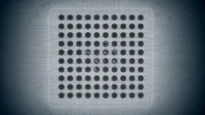
Evaluate BGA solder-joint voids by their size, location, distribution and applicable requirements. Review paste, stencil, reflow and X-ray evidence before choosing corrective actions.
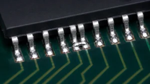
Trace unintended solder connections to printing, placement, board geometry or process conditions, then verify a controlled correction before the next assembly run.
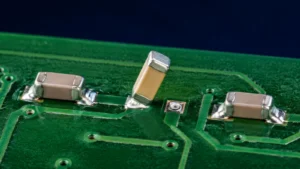
Understand why two-terminal SMT components lift during reflow and use a structured workflow to distinguish design, printing, placement and material contributors.
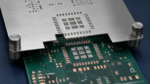
A practical stencil review covering thickness, aperture geometry, paste release and mixed-component requirements, with the inputs needed before SMT production.
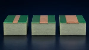
Choose PCB copper by layer with a clear view of conductor geometry, finished thickness, via transitions and manufacturing constraints. Includes a practical review checklist.
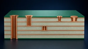
A manufacturing-focused comparison of through, blind, buried and microvia structures, with via-in-pad considerations and the inputs needed to review a multilayer interconnect.