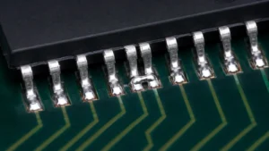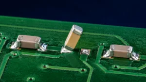
Solder paste stencil design controls how much paste is deposited on each SMT pad and where that deposit sits. Reliable transfer depends on stencil thickness, aperture size and shape, pad geometry, component requirements, solder paste and the printing process working together. Excessive, insufficient or uneven deposits can contribute to bridging, tombstoning, insufficient solder, solder balls and voiding, but a stencil is not the only possible cause of those defects.
Start with the component mix and the most demanding printing features. Then confirm that the proposed stencil can produce repeatable deposits across the assembly. A drawing that looks correct does not replace a controlled print trial.
| Variable | What it influences | Potential risk | Review direction |
|---|---|---|---|
| Thickness | Nominal aperture volume and release geometry | Excess volume or inadequate deposits | Balance the smallest apertures against larger joints |
| Aperture size | Deposit footprint and nominal volume | Oversized deposits; poor release when too small | Check pad relationship and actual transfer |
| Area ratio | Opening area relative to wall area | Low ratios can make release less consistent | Evaluate with paste and stencil process |
| Aperture shape | Paste distribution and local release | Unbalanced or incomplete deposits | Use package-specific geometry and verify printing |
| Local thickness steps | Different volume demands on one stencil | More complex tooling and printing | Use only where the component mix justifies it |
What a Solder Paste Stencil Does
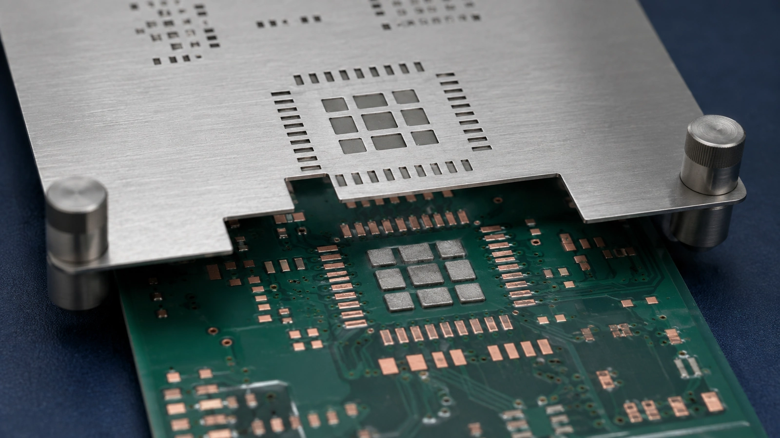
A solder paste stencil meters paste through openings aligned with the PCB’s SMT pads. The printer moves paste across the stencil, fills the apertures and separates the board from the stencil, leaving deposits for component placement.
The paste-layer artwork describes the intended openings, but the manufactured stencil and printing setup determine how that intent becomes a deposit. Board support, stencil contact, aperture condition and separation behavior all affect the result.
Keep copper pads, solder-mask openings and paste apertures distinct. They serve different purposes and need not have identical geometry. Copying a solder-mask layer into a stencil file can introduce unwanted openings or unsuitable deposit sizes. Use the correct assembly side and verify the data revision before tooling.
How to Choose Stencil Thickness
Stencil thickness must balance paste-volume requirements with the ability to release paste from the smallest apertures. A thicker foil increases nominal volume for a given opening, while also increasing the aperture wall area that paste must separate from.
A thinner stencil can support fine-feature release but may provide too little paste for some larger joints. Connectors, power components and large pads can therefore create a different volume demand from small passive components or fine-pitch ICs on the same board.
Identify which features constrain the choice rather than selecting a familiar thickness for every assembly. Review package recommendations, the chosen paste, aperture geometry and the intended print process. If the demands conflict, compare aperture changes and a qualified local-thickness solution before compromising all deposits.
Thickness is a controlled tooling parameter. Record the approved value and any local steps with the stencil revision, so a repeat order does not quietly substitute a different process assumption.
Aperture Size and Shape Control More Than Volume
Aperture dimensions determine both the intended deposit footprint and the geometry available for paste release. Reducing an opening may help control excess paste, but an excessive reduction can make the aperture harder to print consistently.
Review the relationship to the actual copper land and component termination. The preferred opening may match, reduce or otherwise modify the pad footprint depending on package requirements and the qualified process. There is no universal reduction percentage suitable for every component.
Rounded corners can avoid sharp geometric features and may improve release behavior in an appropriate stencil process. Home-plate and other modified apertures redistribute paste rather than simply shrinking it uniformly. Use them to address an identified joint or deposit requirement, not as an automatic modification to every passive footprint.
For paired passive pads, examine the balance between the two deposits. For a row of fine-pitch leads, examine separation between neighboring deposits as well as volume. The relevant question is where the paste will be after printing and placement, not only the opening’s total area.
Area Ratio: Opening Area Divided by Wall Area
Stencil area ratio compares the aperture opening area with the area of its walls. It is useful because paste must release from those walls as the stencil separates from the PCB.
For an ideal straight-wall aperture, area ratio = A / (P × t), where A is opening area, P is aperture perimeter and t is stencil thickness. Use consistent units. For a rectangular opening with length L and width W, this becomes LW / [2(L + W)t]. For a circular opening of diameter D, it becomes D / (4t).
These are geometric relationships, not acceptance limits. They explain why making a stencil thicker or making an aperture smaller can reduce release margin. Irregular shapes should be assessed using their actual geometry rather than a convenient bounding rectangle.
Indium’s powder and stencil design guidance treats area ratio as an important printing parameter. Any numerical guideline must still be interpreted with the paste, aperture wall condition, stencil technology and printing process. A favorable ratio does not guarantee a good deposit, and a difficult ratio requires process evidence rather than an unsupported promise.
Area Ratio Is Different From Aspect Ratio
Aperture aspect ratio commonly compares opening width with stencil thickness. Area ratio includes the complete opening area and perimeter, so it gives different information about wall contact.
A long narrow slot illustrates the distinction: considering width alone does not fully describe its opening-to-wall relationship. Use the definitions supplied by the stencil or package guidance, especially when an irregular shape is involved.
Also separate both ratios from transfer efficiency, which compares measured deposit volume with nominal aperture volume. An aperture’s ideal volume is its area multiplied by thickness; the printed paste does not necessarily reproduce that volume exactly. Inspect actual deposits to determine what the process delivers.
Fine-Pitch Components Set Printing Constraints
Fine-pitch ICs, small passives, QFN packages and some BGA patterns can constrain stencil design because their openings must remain separated and release consistently. The smallest feature may be more demanding than the average feature on the board.
Check the exact package variant and manufacturer assembly guidance. Similar package names can hide different land patterns or solder-volume needs. For BGA components, account for the package’s existing solder-ball construction rather than assuming the paste must supply the entire joint volume.
Review paste suitability with its supplier and the assembly process owner. Changing powder type or flux system affects more than aperture filling and should not become an unreviewed substitute for correcting geometry. The stencil decision should remain linked to a defined material and process combination.
QFN Thermal Pads Need a Separate Volume Review
A single full-open aperture over a large thermal pad may deposit too much paste relative to the surrounding joints. Excess deposit can contribute to component float and alter the final joint geometry.
Segmented or window-pane openings divide the paste deposit and can help manage distribution and outgassing. Their pattern and total coverage still depend on the package, pad, via arrangement, paste and assembly process.
TI’s QFN layout guidance illustrates segmented thermal-pad stencil openings for its example package. Apply the guidance for the actual device rather than transferring one example’s dimensions to every QFN. Voiding is influenced by several factors, so segmentation is not a guarantee of a particular void level. Detailed QFN attachment and void acceptance require their own review.
When Step Stencils Are Useful
A step stencil provides different local foil thicknesses. A step-up region can supply more nominal volume, while a step-down region can support smaller printing features.
This may help when a mixed-component assembly cannot satisfy both large and small joint requirements with one uniform thickness. It is not necessary for every board containing different package sizes.
Steps introduce tooling and printing constraints. Their location relative to apertures, the printing direction and the support arrangement need review with the stencil supplier and assembly team. A local volume improvement is not useful if the step disrupts printing elsewhere. Validate the proposed arrangement on the intended equipment before releasing it as the production solution.
Connect Stencil Findings With the Actual Defect
A stencil-related defect investigation should begin with the measured deposit, then connect that evidence to the post-reflow symptom.
- Bridging: excessive or displaced deposits can contribute to an unwanted connection, but placement and process conditions also matter. Use the solder-bridging corrective workflow for the full investigation.
- Tombstoning: unequal deposits can contribute to unbalanced wetting at a two-terminal component. The tombstoning diagnosis and prevention guide covers the other causes.
- Insufficient solder: an undersized opening or inconsistent release may reduce deposit volume.
- Solder balls or beads: deposit position, volume and subsequent processing can leave solder outside the intended joint.
- Voiding: paste distribution is one variable among package geometry, material and reflow conditions.
Do not change the stencil simply because a defect appears after reflow. A good print followed by incorrect placement calls for a different corrective action from a consistently missing deposit.
Review the Stencil Before Production
A useful review compares the intended joint requirements with both the tooling design and evidence from the printing process.
- Confirm the release data. Match PCB, paste layer, BOM and assembly revisions, including the correct board side.
- Identify limiting packages. Flag small apertures, fine-pitch rows, large thermal pads and high-volume joints.
- Review thickness and openings together. Check dimensions, shape, area ratio and any local thickness changes.
- Check process compatibility. Confirm paste selection, board support, printer setup, stencil cleaning and separation requirements.
- Inspect trial deposits. Use suitable measurement or solder paste inspection to assess volume, position, consistency and missing deposits.
- Verify the assembled result. Review the relevant joints after placement and reflow, not just the appearance of the printed board.
- Release the proven revision. Record accepted changes and retain the evidence needed for repeat builds.
A single acceptable print does not establish repeatability. Include relevant restart or interruption conditions in the evaluation and look for feature-specific trends. Change one controlled variable at a time where practical, so an improvement can be traced to its cause.
The DFM, DFA and DFT review framework places stencil feasibility within the wider production decision. The turnkey assembly workflow explains how approved data progresses into manufacturing.
Information Required From the Customer
Provide enough information to identify the required deposits and the assembly conditions:
- Gerber or ODB++ data with clearly identified paste layers and revision.
- BOM with exact component part numbers and package information.
- Assembly drawing and Pick and Place data for the relevant side.
- Package-specific assembly guidance, particularly for QFN, BGA or unusual terminations.
- Existing stencil thickness, aperture data and any step-stencil requirements.
- The intended paste and SMT process, including relevant reflow constraints.
- Known print measurements, defect evidence or special joint requirements.
If the stencil supplier is permitted to modify the paste artwork, identify who approves those changes. Retain the accepted manufacturing file alongside the design release rather than allowing an undocumented local version to become the repeat-build reference.
Settle Paste-Transfer Requirements Before SMT Production
Excel Circuit’s in-house design engineering and SMT assembly services connect the package and PCB data with practical production inputs. Stencil review can identify unresolved assumptions before tooling and setup.
Send your paste layer, BOM and assembly data for a stencil and solder-paste requirement review. Include any existing aperture changes and print concerns so the review starts from the actual build definition. Submit your stencil and assembly inputs.