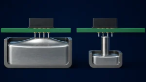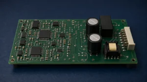
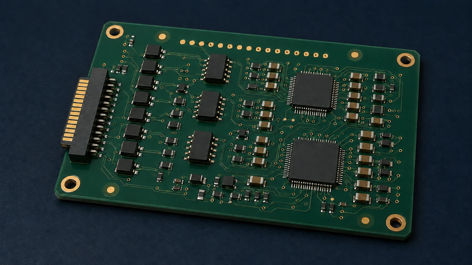
PCB Design for Assembly (DFA) makes a board easier and more repeatable to place, solder, inspect, test, rework and handle. Good PCB assembly design guidelines address avoidable process complexity before production. They do not replace electrical performance, safety or mechanical requirements: the goal is an assembly route that satisfies those requirements without relying on undocumented workarounds.
Use this checklist early, then review the actual package data and proposed assembly equipment with manufacturing. Clearance depends on the operation and its access envelope; one spacing value cannot represent every placement head, soldering nozzle, probe or rework tool.
| DFA area | What to review | Common assembly risk |
|---|---|---|
| Component spacing | Placement and rework access | Tool collision or inaccessible joints |
| Orientation | Polarity and package direction | Placement or inspection errors |
| Fiducials | Board and panel alignment references | Unreliable machine registration |
| Board edge | Conveyor, clamp and tooling space | Handling interference |
| Land pattern | Exact package compatibility | Poor joint geometry |
| Solder mask | Intended pad isolation | Unwanted solder connections |
| Thermal pad and vias | Paste balance and via treatment | Float, solder loss or voiding |
| Test access | Probe approach and fixture clearance | Incomplete validation |
| Tall or heavy parts | Support and handling stability | Movement or mechanical interference |
| Through-hole parts | Insertion and secondary soldering access | Unplanned extra operations |
What Is PCB Design for Assembly?
PCB DFA is an assembly-focused review of how the physical layout, components and instructions will pass through production. Fabrication DFM asks whether the bare board can be manufactured consistently. DFA asks whether the parts can be fitted and joined consistently. DFT contributes the access and procedures needed to verify the resulting circuit.
The DFM, DFA and DFT review framework explains those boundaries. In a practical DFA review, identify the operation affected by each concern, the evidence needed and the person authorized to approve a change. “Manufacturing to adjust” is not a complete disposition when the adjustment changes a controlled footprint or mechanical interface.
Review Component Placement and Spacing by Operation
Component spacing must support the tools and process used around the part, not just prevent two component outlines from overlapping. Compare the placed component envelope with neighboring heights, placement-nozzle access, inspection sightlines and the intended rework approach. Include package tolerances and protruding connector features.
A tall connector can block a tool that needs to approach a small device beside it. A closely packed group may be placeable but difficult to inspect or replace. Ask manufacturing to identify the limiting operation and evaluate moving, rotating or resequencing the affected part. Keepout zones should name their purpose so a later layout change does not unknowingly remove a necessary access path.
Preserve critical electrical relationships such as short high-frequency paths and decoupling placement. Where access conflicts with performance, compare realistic alternatives rather than moving components only to satisfy a generic spacing checklist.
Make Orientation Clear Without Overriding Circuit Needs
Consistent orientation can simplify placement verification and reduce interpretation errors, especially for polarized capacitors, diodes, LEDs, IC pin-one markings and connectors. Use consistency where it fits the circuit and mechanical layout, while making exceptions explicit.
Confirm polarity against the component manufacturer’s convention, not a remembered package appearance. The footprint, silkscreen, assembly drawing and placement library should tell the same story. A diode symbol or connector key that conflicts with a pin-one mark requires resolution before release. Do not rotate a device for visual uniformity when doing so would compromise routing, signal integrity, thermal behavior or mating access.
Provide Fiducials for the Actual Alignment Strategy
Fiducials provide recognizable references that assembly equipment can use to locate the PCB or panel. Global fiducials support overall registration; local fiducials may help with demanding fine-pitch or BGA placement, depending on the equipment and board design.
Review their visibility, contrast and surrounding clearance with the assembler. Features hidden by a clamp, component or carrier cannot serve the intended alignment step. For panels, distinguish panel registration from the positions of individual circuits and confirm which references the placement program will use. Specify the required geometry through the assembler’s approved guidance rather than importing unsupported universal dimensions.
Reserve Board-Edge and Tooling Access
Board edges must accommodate the proposed conveyor, clamps, supports and any panel rails. An edge connector may satisfy the enclosure drawing while occupying the space needed to transport the board. Review both requirements before deciding whether a carrier, rail or different orientation is needed.
Check depanelization access and the locations of components vulnerable to mechanical strain during separation. Identify when temporary rails are removed relative to insertion, testing and final assembly. Detailed panel design belongs in a dedicated panelization review; the DFA decision here is whether the handling route remains feasible at every stage, including after rails or supports are gone.
Match Land Patterns to the Exact Component
Land-pattern review starts with the exact manufacturer part number and package variant. Compare the approved footprint with lead dimensions, package tolerance, recommended land pattern and the intended soldering method. Similar package names do not guarantee interchangeable mounting geometry.
Inspect custom or modified footprints explicitly. A change intended to improve routing may alter solder-joint formation or shift the component’s seated position. Review copper, mask and paste together while preserving their separate purposes. Record the source drawing and approved revision so later component substitutions trigger an appropriate review instead of silently inheriting an unsuitable footprint.
Coordinate Solder Mask and Paste Layers
Solder mask defines intended exposed areas and helps separate adjacent solderable features; the paste layer defines where paste will be deposited through the stencil. Neither layer should be treated as an unchecked copy of the copper geometry.
Review whether mask registration and available separation support the proposed pad layout. Then check the paste openings against the selected stencil strategy and package requirements. The stencil thickness and aperture design guide covers paste-transfer decisions in detail. Where adjacent pads or excess deposits create a risk, the solder-bridging diagnostic guide provides the supporting defect context.
The release question is whether the design layers express a coherent assembly intent. Detailed solder-mask rules and full printing-process optimization should remain separate reviews with the appropriate fabrication and assembly input.
Review BGA and Fine-Pitch Assembly Constraints
BGA and fine-pitch components connect escape-routing choices to assembly outcomes. Review pad geometry, routing-related vias and the treatment of openings that could divert solder. A route that works electrically can still create an unfavorable soldering surface if the via treatment is unspecified.
Use the PCB via and via-in-pad comparison to distinguish the interconnect options, then confirm the actual fabrication treatment. Include placement alignment, board support and hidden-joint inspection in the assembly plan. X-Ray may support the required structural checks, but it does not establish electrical function. This review identifies the constraints; it does not replace a BGA fanout or voiding investigation.
Balance QFN Center Pads and Perimeter Joints
QFN exposed-pad assembly depends on balancing center-pad solder with the perimeter joints and the package’s intended standoff. Thermal vias, solder loss into openings and paste distribution affect that balance. A generous center deposit is not automatically a safer design.
Review the exact package guidance, thermal/electrical pad role and specified via treatment together. The QFN thermal-pad, via and stencil guidelines explain those package-specific decisions. In the overall DFA checklist, confirm that the QFN review is complete and that its approved changes are reflected in the released layers.
Design Through-Hole Parts Into the Assembly Route
Through-hole design must connect component leads, finished holes and soldering access. Review the lead geometry and tolerance against the finished-hole requirement, insertion method and component seating. A nominal drill callout alone does not establish that the supplied lead will fit the finished plated hole.
Consider orientation, lead protrusion, nearby bottom-side components and support for tall or heavy parts. The soldering tool, wave pallet or selective nozzle must reach the joints without contacting protected features. Review the mixed SMT and through-hole assembly sequence before freezing access around connectors, relays or other late-installed parts. A feasible insertion step must also leave the later inspection and test steps feasible.
Protect Inspection and Test Access
Inspection and test access should be designed before the board becomes densely populated. Check whether visible joints remain observable after tall components are installed and whether hidden joints have an appropriate inspection strategy. An AOI program cannot compensate for a feature that the optical system cannot see.
For electrical testing, review test-point locations, probe approach, fixture supports and connector access against the planned method. Avoid obstructing a probe with a component that is added before the test stage. The PCB assembly testing-method comparison helps distinguish inspection coverage from electrical or functional evidence. State which tests are required and identify unresolved coverage gaps before release.
Consider Reworkability as a Controlled Recovery Need
Reworkability means preserving a realistic way to access and replace a part when authorized. Review nearby heat-sensitive components, connector obstructions and the space needed for heating, removal and cleaning operations. A part that can be assembled automatically may still be impractical to replace without disturbing its neighbors.
Rework is not the primary design objective, and every component does not need unrestricted access at the expense of product performance. Focus on high-risk, high-value or service-relevant parts and document any accepted limitations. Do not assume that repeated heating is harmless; the applicable component and board constraints still govern a repair plan.
Make the Assembly Documentation Unambiguous
The assembly package must identify what to install, where to install it and which exceptions apply. Reconcile BOM manufacturer part numbers, Pick and Place data, assembly drawings, polarity notes and special instructions. List DNP/DNI positions explicitly, particularly when multiple product variants share a PCB.
Use the controlled production-package checklist to organize the release. Confirm that an approved footprint or orientation correction appears in every affected output. A drawing annotation cannot safely compensate for a contradictory placement file unless the change is formally controlled and transferred into the build instructions.
Complete DFA Checklist for Production Release
Assign each item a result, evidence reference and owner. Mark an item not applicable only when its absence is understood. Open issues need a disposition before the build is treated as released.
- Placement: component envelopes, heights, polarity and operation-specific access reviewed.
- Footprints and pads: exact packages, tolerances, modified lands and component substitutions checked.
- Solder mask and paste: intended isolation, aperture strategy and approved layer changes reconciled.
- BGA/QFN: via treatment, exposed-pad strategy, alignment and hidden-joint inspection addressed.
- Through-hole: finished holes, leads, seating, protrusion, support and solder access confirmed.
- Tooling: conveyor edges, clamps, supports, rails and separation sequence feasible.
- Test: probe access, connector access, coverage and functional requirements agreed.
- Documentation: compatible revisions, placement data, polarity, options and DNP/DNI instructions released.
- Rework: critical parts accessible or limitations explicitly accepted.
- Production release: engineering and manufacturing agree the remaining constraints, build route and approval responsibility.
Use the checklist to close decisions, not just to collect ticks. For example, an edge-clearance issue is closed when the approved handling solution and its effects on testing and separation are documented, not when someone notes that a fixture could probably be made.
Information Required From the Customer
Provide Gerber or ODB++ data, BOM, Pick and Place file, assembly drawing, stackup and drill data from a controlled release. Include component datasheets for unusual or modified packages, the DNP/DNI list, mechanical constraints and expected production quantity.
Add test requirements and any restrictions on soldering, handling or component substitution. Identify which layout features are electrically or mechanically fixed and who can approve changes. This lets the review distinguish design changes from process accommodations and avoids an apparently simple manufacturing adjustment creating a new product problem.
Request an Assembly-Readiness Review
Excel Circuit connects in-house PCB design engineering, component sourcing and in-house SMT assembly with qualified PCB manufacturing resources through its turnkey PCBA support. Through-hole and secondary assembly requirements should be reviewed for the particular job and proposed process route.
Submit your assembly-readiness review inputs with the PCB files, BOM and placement data before releasing the design to PCBA production. Include the mechanical constraints and test expectations so the review can resolve access, documentation and process-sequence questions together.