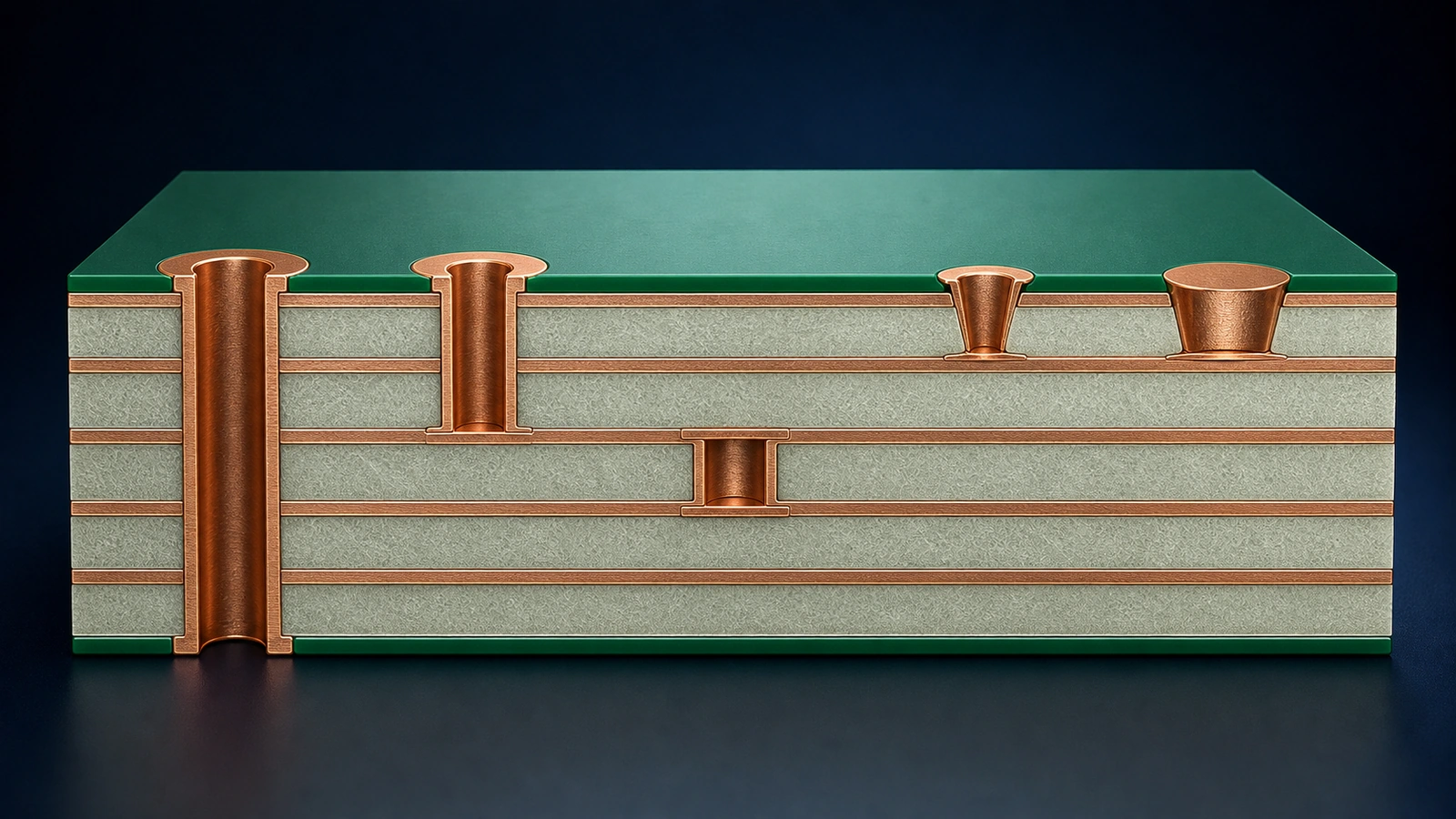
PCB via types describe different ways to connect conductive layers. Through-hole vias pass through the board; blind vias connect an outer layer to internal layers; buried vias connect internal layers without reaching either outer surface. Microvias are short interconnect structures commonly laser-drilled in HDI construction. Via-in-pad describes a via’s location inside a component pad, rather than a separate layer-span category.
Select a structure from the required connections, routing density, BGA pitch, stackup, signal performance and manufacturing constraints. Cost and reliability depend on the construction and process behind the label. A board can use several via types, and a microvia can also be blind and located in a pad.
| Via type | Layers connected | Main advantage | Main limitation | Typical use | Manufacturing impact |
|---|---|---|---|---|---|
| Through-hole | Full board span; selected layers connect | Common construction | Occupies space across the stack | General multilayer routing | Mechanical drilling and hole plating |
| Blind | Outer to internal layers | Frees routing below its span | Depth and access constrain construction | Dense surface routing | Controlled-depth or buildup process |
| Buried | Internal layers only | Preserves outer-layer area | Must be formed before enclosure | Dense multilayer connections | Subassembly processing and lamination |
| Microvia | Short layer span in the buildup | Supports compact interconnects | Structure and interfaces require qualification | HDI and fine-pitch routing | Usually laser drilling and staged processing |
| Via-in-pad | Depends on the underlying via | Connects directly from a component land | Pad surface must suit assembly | Selected BGA or thermal pads | Fill, cap and plating requirements may apply |
Through-Hole Vias: The Common Starting Point
A through-hole via is a plated connection drilled through the completed board thickness. It can connect selected layers along that span; clearance features isolate layers that should not connect to it.
This construction is widely used because drilling and plating through the stack are established fabrication operations. It is often a sensible starting point when component pitch and routing area allow it. A plated through via is not the same as a component mounting hole, even though both may use related fabrication processes.
The routing cost is its full-depth presence. Pads, holes and clearances consume space on layers where the signal may not need a connection. Unused barrel length can form an electrical stub. On a dense multilayer board, that occupied area may make another via structure worthwhile even if the through via itself is straightforward to manufacture.
Blind Vias: Outer Layers to Internal Layers
A blind via reaches from an outer surface to one or more internal layers without passing through the whole finished board. It leaves the remaining layers available for other routing.
Blind vias may use different drilling and buildup approaches depending on their depth and construction. They are not all microvias. A mechanically formed blind structure and a short laser-drilled microvia can share the same broad outer-to-inner description while requiring different fabrication plans.
Define the actual start and stop layers. The fabricator must be able to create, clean and plate the connection at the appropriate stage. Some constructions require sequential lamination; others use a different controlled process. Do not assume that any pair of layers shown in a routing tool can be connected economically or reliably in the final stack.
Buried Vias: Connections Inside the Board
A buried via connects internal layers and is not exposed on either outer surface of the completed PCB. Its hole and plating must be formed while the relevant subassembly is still accessible, before later layers enclose it.
The advantage is routing density: internal connections can be made without consuming a surface pad location or extending through unrelated outer layers. This can help when several interconnect groups compete for space.
The manufacturing consequence is an ordered construction sequence. Drilling, plating, inspection and any required fill must fit the subassembly and lamination plan. An apparently small layer-span change can alter that sequence. Review buried vias with the complete stackup rather than requesting them as an isolated drill option after layout completion.
Microvias: Short Interconnects for HDI
A microvia is a short interconnect structure commonly made by laser drilling in an HDI buildup. It connects a shallow span and supports compact routing where a larger conventional via would consume too much space.
Microvias are often created as dielectric and copper layers are added in stages. The material, target pad, drilling process, cleaning and metallization must work together. The word “microvia” does not authorize a universal diameter or depth-to-diameter ratio for every supplier and material.
Choose the minimum buildup complexity that achieves the connection. A microvia to an adjacent layer may solve a local escape problem; connecting deeper into the board can require additional structures and processing. Confirm the actual layer sequence with the manufacturer before fixing the component escape geometry.
Reliability review should include the intended assembly thermal history and product environment. Passing a basic continuity check on the bare board does not, by itself, establish that every microvia interface will remain sound after assembly and service stresses.
Via-in-Pad: Location and Surface Condition Matter
Via-in-pad places the interconnect within a component’s solder land. It can shorten the route out of a fine-pitch pad or provide a thermal connection, but it must be specified with the underlying via structure and the required finished pad surface.
An open hole in a solder pad can draw solder away from the joint or create an uneven assembly interface. Tenting with solder mask is not automatically equivalent to a filled, capped and plated-over structure. VIPPO identifies via-in-pad plated over; the required filling, planarization and cap construction must be agreed with the fabricator.
Whether a particular pad needs that process depends on its function and assembly requirements. Do not treat every thermal-pad via and every fine-pitch BGA pad as the same problem. Fill material and finished surface need explicit review rather than a generic note saying “fill vias.”
The dedicated via-in-pad and VIPPO design guide covers pad construction and soldering implications in detail. Here, the selection question is whether placing the connection inside the pad justifies those process requirements.
Stacked vs Staggered Microvias
Stacked microvias align successive interconnects vertically. Staggered microvias offset them laterally and connect through copper on an intermediate layer. Stacking saves routing area; staggering requires lateral room.
The two arrangements create different interfaces and process demands. A stacked structure relies on the quality of successive target and fill interfaces, while the complete reliability outcome also depends on material, geometry, process control and thermal loading. Neither label alone guarantees reliability.
IPC’s microvia reliability warning identifies weak-interface concerns in certain structures and limitations of traditional inspection. That warning supports requiring construction-specific evidence; it should not be interpreted as proof that every stacked microvia is defective.
Ask what qualification or validation evidence supports the proposed stack and assembly conditions. If routing permits a simpler arrangement, compare it before accepting extra stacked levels. Do not transfer a reliability result from one tested material and geometry to a different construction without review.
How Via Selection Changes BGA Fanout
BGA pitch affects the space available for pads, clearances and escape traces, but pitch alone does not determine the via type. Ball assignment, routing density, available layers and manufacturing geometry also matter.
A through-via approach may be sufficient when the escape channels fit. Blind vias or microvias can free routing space when the full-depth hole blocks the required paths. Via-in-pad may create a direct exit where an offset connection will not fit, at the cost of a more demanding pad process.
Make the decision with the ball map and stackup together. Adding layers does not necessarily recover routing area consumed by unsuitable via structures. Use the BGA fanout and escape-routing guide for the detailed routing strategy; avoid choosing a fabrication process from package pitch alone.
What High-Speed Signals Need From a Via
A signal via changes the interconnect geometry and may introduce unused barrel length, or a stub. It can also move the signal to a layer with a different reference plane.
Review the return-current transition as well as the signal connection. Appropriate stitching connections may be needed where the reference arrangement changes, but placing a nearby ground via does not solve every reference-plane transition. The correct path depends on which planes provide the reference and how they are connected.
Shorter spans can reduce unnecessary barrel length, yet a blind via or microvia is not automatically an optimized high-speed transition. Pad geometry, clearances, reference continuity and the channel requirement still need consideration. The stackup and reference-plane planning guide provides the wider layer context.
Why Via Choices Affect PCB Cost
Via cost follows the required operations: mechanical or laser drilling, plating, filling, planarization and lamination stages. The combination of structures matters more than the name of one via.
A buried connection can add subassembly work. Multiple buildup stages can increase processing and inspection requirements. Via-in-pad can add surface preparation that a nearby open via would not require. A dense construction may also narrow the range of qualified manufacturing resources.
Compare complete constructions against the same functional requirements. A more capable via structure may reduce routing congestion or layer count, but those savings are project dependent. Request the process assumptions behind each option instead of using a fixed cost percentage for “HDI” or “microvia.”
How to Select the Right Via Structure
Select vias by matching each required connection to a manufacturable span, then checking the board-level consequences.
- List the connections. Identify start and stop layers, critical nets and any component-pad constraints.
- Try the simpler construction. Check whether through vias meet routing density and electrical needs before introducing additional buildup stages.
- Resolve the dense regions. Use the BGA ball map, pitch and escape space to identify where blind, buried or microvia structures are justified.
- Agree on the stackup. Confirm drilling access, lamination sequence, layer spans and fill requirements.
- Check assembly and reliability. Review pad surfaces, thermal processing and evidence for the proposed interconnect construction.
- Compare the whole project. Assess electrical performance, layer count, manufacturing complexity and production cost together.
- Release consistent data. Align drill files, span definitions, stackup and drawing notes before manufacture.
For example, a board may use through vias for ordinary routing and a limited microvia region for a dense component. That selective use can be worth comparing with an unnecessarily complex board-wide structure. It still requires a coherent fabrication sequence; local layout simplicity does not eliminate whole-board processing requirements.
Information Required From the Customer
A via review needs enough information to reconstruct the intended connections and assembly interfaces:
- Gerber or ODB++ data and the relevant design revision.
- Drill data with clear plated/non-plated distinctions and layer-span assignments.
- The proposed stackup, layer count and finished board thickness.
- BGA pitch and ball-map information for density-driven decisions.
- Required through, blind, buried or microvia structures, including stacked or staggered arrangements.
- Via-in-pad locations and explicit fill, cap or plating-over requirements where applicable.
- Impedance and signal-transition requirements for critical nets.
- Fabrication drawing, reliability expectations and relevant assembly thermal constraints.
Identify undecided items as questions. A drill file with no span map cannot reliably communicate a complex multilayer construction, and a stackup sketch cannot replace the finished pad requirements.
Review the Interconnect Before Committing to Fabrication
Excel Circuit’s in-house design engineering can coordinate interconnect decisions with qualified HDI PCB manufacturing resources. Its in-house SMT and turnkey PCBA support also provide the assembly context needed when a via occupies a solder pad.
Send your PCB data, drill information and stackup for a via-structure and manufacturability review. Identify dense components, critical transitions and fill requirements so the review addresses the connections that drive the construction. Submit your PCB data and via requirements.