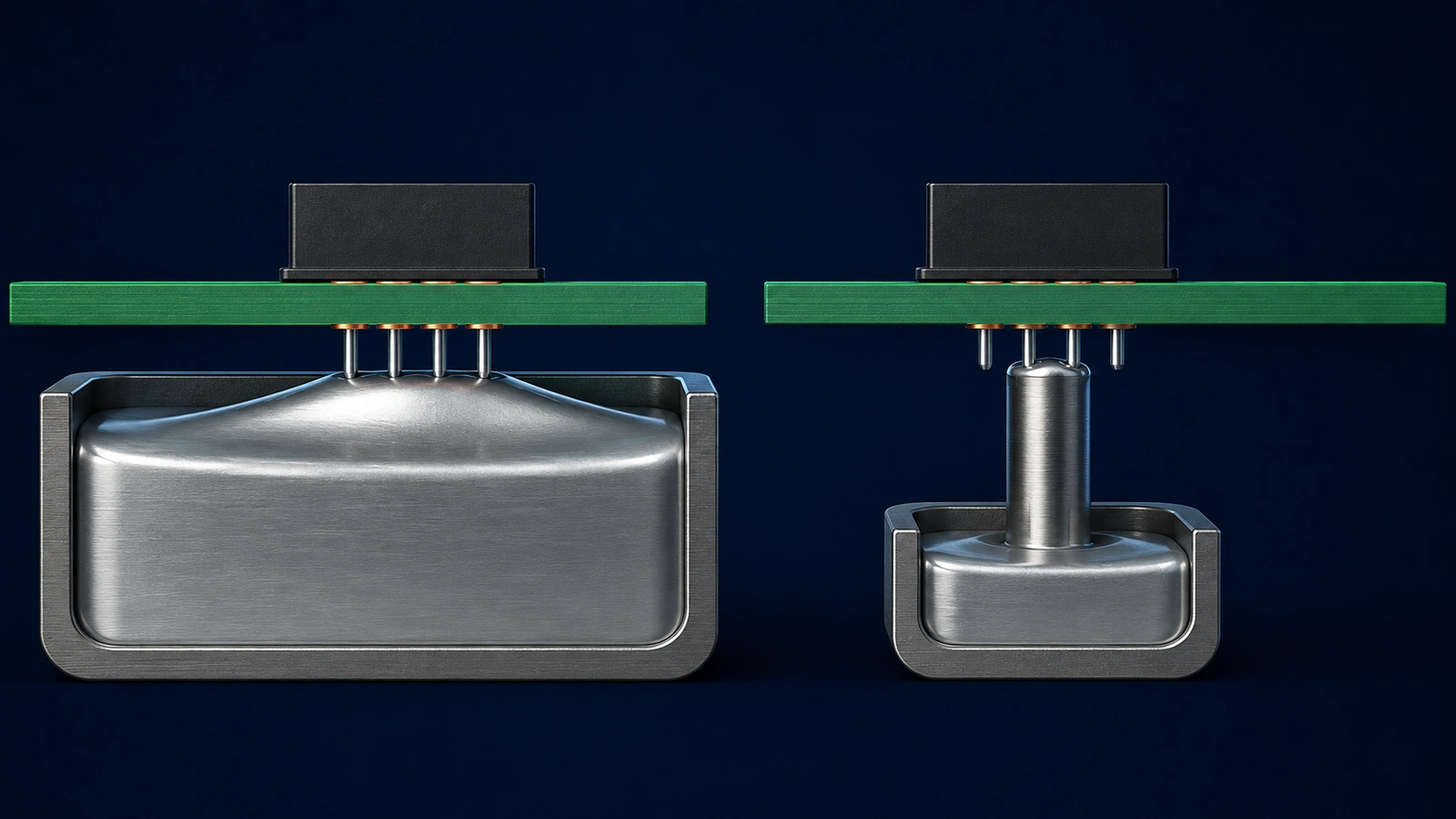
Wave soldering exposes the intended solder side of an assembly to a broader solder wave, while selective soldering targets specific through-hole joints or areas. The better fit depends on component density, solder-side SMT, access, quantity, masking, thermal restrictions, board geometry and repeatability requirements. Neither process is always superior, and neither can compensate for an incompatible layout without an approved design or process change.
First establish which routes can reach and solder the required joints safely. Then compare the complete production route, including setup, insertion, tooling, inspection and changeover, rather than choosing only from a machine cycle-time claim.
| Factor | Wave soldering | Selective soldering |
|---|---|---|
| Solder coverage | Broader exposed area | Targeted joints or areas |
| Typical fit | Accessible, compatible joint populations | Mixed populations needing local control |
| Solder-side SMT | Compatibility and protection require planning | Often accommodated if nozzle access remains |
| Masking | Pallets or masking may be needed | Less broad masking may be needed; tooling still matters |
| Flexibility | Constrained by exposed geometry and solder flow | Local path and joint-group control |
| Cycle time | Can be efficient for suitable populations | Sequential paths can take longer; equipment dependent |
| Process preparation | Flux, preheat, transport and tooling setup | Flux, preheat, nozzle, path and support setup |
What Is Wave Soldering?
Wave soldering forms joints by bringing the intended solder side into contact with a controlled wave of molten solder. Fluxing prepares the solderable surfaces, and preheating supports the process before solder contact. The board’s geometry, thermal demand and movement through the process influence the resulting joints.
For through-hole connections, solder must wet the intended lead and plated-hole surfaces under the agreed requirements. The process is not simply a bath that every populated board can pass through. Bottom-side components, connector features and areas that must remain unsoldered determine whether direct exposure is suitable or whether protection and tooling are needed.
What Is Selective Soldering?
Selective soldering applies solder to chosen joints or regions, commonly through a controlled nozzle or small solder wave. Flux application, preheating and solder contact are coordinated with the target locations. The machine may move the board, the soldering system or both, depending on its design.
Nozzle geometry and programmed paths must suit the accessible joint population. Localized soldering does not mean that heating is confined perfectly to a single pin or that the rest of the assembly stays cold; some systems use broader preheating. Review the actual equipment configuration instead of assuming a universal process from the word “selective.”
Board Layout Determines Which Routes Are Feasible
Layout suitability starts on the solder side. Map the through-hole joints, bottom-side SMT, protruding leads, connectors and mechanical obstacles. Identify which features can contact solder and which need protection. A top-side assembly image alone is insufficient for this decision.
Wave processing requires a compatible exposure pattern and workable flow around the relevant features. Selective processing requires access for the nozzle and its movement, as well as the fluxing and support arrangement. A tightly packed underside can make either route difficult. Review the approach and exit paths around connectors and tall obstacles rather than checking only the space directly beneath a joint.
Consider the assembly state at that step. A later-installed bracket may not matter during soldering, while a component already present can block access even if it is not part of the through-hole population.
Production Volume Changes the Economics, Not the Physics
Volume influences how setup, tooling and cycle time contribute to cost, but it does not make an inaccessible joint accessible. A compatible wave route can process broad populations efficiently. A selective route may avoid extensive masking or separate manual work on a mixed board.
Do not classify selective soldering as inherently low-volume or wave soldering as inherently high-volume. The number and distribution of joints, repeat demand, changeovers and actual machine configuration matter. Some selective systems address groups of joints or use parallel arrangements; those capabilities must be confirmed rather than assumed.
Ersa’s technical discussion of wave and selective process combinations illustrates why joint distribution and equipment configuration affect throughput. It is an equipment-specific example, not evidence that Excel Circuit operates that system or that one volume threshold selects a process.
Compare Masking and Tooling as Part of the Route
Wave pallets or masking can protect components and expose selected regions to solder. Their design must preserve joint access, adequate heating, board support and repeatable loading. A pallet is therefore a process element, not just a cover that makes any board wave-compatible.
Selective soldering often reduces the need for broad masking, but nozzle clearance, support fixtures and programming remain important. Check whether long leads or nearby components interfere with the chosen nozzle and whether a fixture blocks the flux or solder path. Include loading, unloading, cleaning and maintenance implications in the review where relevant.
Compare the whole tooling plan, including changes needed for product variants. Avoid deciding that a process is cheaper merely because its quoted setup line is smaller while additional manual handling or inspection remains unaccounted for.
Review Thermal Exposure at the Component and Board
Wave soldering typically involves broader solder-side exposure, while selective soldering provides local control of solder contact. Both require a thermal process compatible with the board, joints and components. Local solder application can still heat a connector body or neighboring part through the board and leads.
Obtain the relevant supplier restrictions for sensitive plastics, connectors and other affected components. Distinguish solder contact conditions from measured component-body temperature. Consider the earlier SMT reflow history and the cumulative implications of additional operations.
A difficult joint connected to substantial copper may require different process attention from a lightly connected joint. Manufacturing should establish the necessary profile and contact conditions against the real assembly. Do not solve that question with an unsupported universal temperature or dwell time.
Joint Consistency Depends on Controlled Setup
Consistent joints depend on repeatable flux application, preheat, solder contact, material condition and access. Both processes can produce acceptable joints when the design and controlled process are appropriate. Neither process name guarantees better workmanship.
Define the variables that need control and the evidence required during setup and repeat builds. For wave soldering, transport and exposure conditions must remain suitable. For selective soldering, nozzle condition, position, path and contact behavior must remain suitable. Component leads, plated-hole solderability and board variation also affect outcomes.
Use representative assemblies to verify the proposed route, then record the approved setup and acceptance requirements. A single acceptable-looking joint is insufficient evidence that every geometry and thermal condition on the board has been addressed.
Design Rules That Influence Process Choice
Through-hole spacing, connector positioning, component height and solder-side population should be reviewed against the chosen process. The critical clearance is the space needed by the actual soldering and tooling arrangement, including its movement and tolerance.
The assembly-focused DFA checklist covers those access decisions. Provide a bottom-side component map and realistic lead protrusion information when seeking process feedback. Moving a connector slightly may simplify the route, but only the responsible design team can approve the effects on mating, routing and mechanical requirements.
Freeze the process-relevant keepouts in the controlled design. Otherwise a later component substitution or underside placement change may invalidate a previously workable nozzle path or pallet opening.
Recognize Defects Without Turning Them Into Process Stereotypes
Bridges, inadequate hole fill, icicles, skips or non-wetted areas can arise when geometry, solderability or process conditions are unsuitable. Thermal damage is another concern when exposure exceeds the applicable component or board constraints. These risks need an investigation tied to the affected joint and process stage.
Do not infer that a bridge proves wave soldering was the wrong method, or that a skipped joint proves selective soldering is inherently unreliable. Review access, flux, heat transfer, lead geometry and solder behavior before deciding on corrective action. Use the customer’s acceptance requirements and the applicable standard and revision; this comparison does not establish a universal solder-fill threshold.
Detailed cold-joint, insufficient-solder and reliability diagnosis belongs in dedicated technical reviews. Here, the relevant selection question is whether the proposed route has a credible way to prevent, detect and control its likely failure modes.
Define Inspection and Testing Before Approving the Process
Visual inspection can verify accessible joint and component features. AOI may support suitable visible checks, but its usefulness depends on access and the inspection program. Where a feature cannot be judged from the visible surfaces, the inspection plan must address that limitation rather than assume a photograph proves internal condition.
Electrical and functional tests answer different questions from workmanship inspection. Use the PCB assembly inspection and testing comparison to establish coverage. Confirm how the selected process will be validated on the first build and monitored on repeat work. Record exclusions and required customer decisions before calling the route production-ready.
When Wave Soldering May Be the Better Fit
Wave soldering may be suitable when the intended joint population is broadly accessible, exposed materials are compatible and any needed masking or pallet is practical. It can be attractive when many joints can be processed efficiently within a stable route.
Confirm that bottom-side components are compatible with the planned exposure or effectively protected. Check that tooling does not create inaccessible or poorly heated regions. Evaluate the labor and handling required around the wave stage, not only the soldering pass. If protection becomes complicated or exceptions require many additional operations, compare another route before committing.
When Selective Soldering May Be the Better Fit
Selective soldering may be preferable when specific through-hole groups need soldering among populated or protected regions and a workable nozzle path exists. Local process control can help accommodate different joint locations or product variants without exposing the whole solder side in the same way.
Confirm access for every target, including closely spaced connectors, long leads and obstacles. Compare the programmed path, setup and handling with the production demand. If sequential processing dominates the route, investigate the actual equipment options or a different layout rather than assuming that “selective” automatically means flexible enough.
To place either choice within the complete build, review the mixed SMT and through-hole process sequence. The selected secondary method must fit the operations before and after it.
A Practical Process-Selection Matrix
Use this matrix to define the next engineering check. It identifies conditions to investigate, not an automatic winner or a substitute for sample validation.
| Board or production condition | Route to investigate | Evidence needed before selection |
|---|---|---|
| Many accessible THT joints | Wave and efficient selective configurations | Exposure compatibility and complete route time |
| Dense bottom-side SMT | Selective access or protected wave route | Nozzle path or feasible pallet openings |
| Few isolated THT groups | Localized soldering options | Setup effort, reach and thermal response |
| Restricted access | Layout change or qualified alternative route | Tool, fixture and movement envelopes |
| Repeat volume with stable design | Compare validated total-route economics | Setup amortization, handling and repeatability |
| Extensive masking | Compare local processing with the protected wave plan | Masking labor, consistency and heating effects |
| Temperature-sensitive parts | Review installation sequence and controlled exposure | Supplier limits and measured assembly conditions |
| Frequent product variants | Compare changeover and tooling flexibility | Program control, fixture compatibility and verification effort |
Information Required From the Customer
Provide Gerber data, BOM, assembly drawing and a clear through-hole component list. Include the bottom-side component map, lead and package information, mechanical restrictions, quantity and expected repeat demand.
State soldering restrictions, thermal limitations and acceptance requirements. Identify whether the layout is fixed or whether engineering changes can be considered. These details let the process review distinguish an equipment-access problem from a component-compatibility problem and compare feasible routes on the same basis.
Choose the Secondary Soldering Route With the Build Team
Excel Circuit supports in-house PCB design engineering, SMT assembly and component sourcing, coordinated with qualified PCB manufacturing resources through turnkey PCBA services. Secondary soldering arrangements should be confirmed for the project; no specific wave or selective equipment ownership is implied.
Submit your secondary-soldering review inputs with the PCB data, BOM and through-hole requirements. Include the bottom-side layout and process restrictions so the team can compare appropriate options before production.