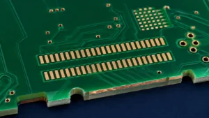
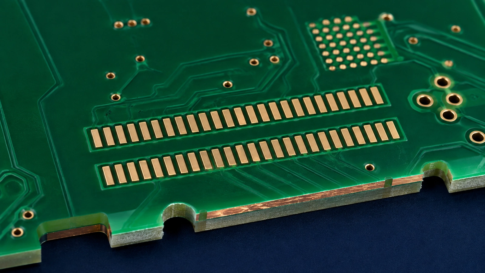
PCB solder mask protects copper, defines exposed solderable regions and helps reduce unintended solder spread. It also provides a protective insulating layer over covered areas. Openings must accommodate component geometry and fabrication registration: poorly designed openings can cause mask encroachment, missing dams, unintended exposed copper, bridging sensitivity and assembly difficulty.
Design the copper, mask and paste layers as related but separate requirements. A suitable opening for one package or fabrication process is not a universal rule. Confirm expansion, web survival and via treatment with the fabricator and assembler before releasing fine-pitch layouts.
| Feature | Purpose | Risk if poorly designed | Review decision |
|---|---|---|---|
| Mask expansion | Set opening relative to copper pad | Encroachment or excessive exposure | Confirm pad definition and registration allowance |
| Mask dam | Separate adjacent openings | Missing web and increased bridging sensitivity | Confirm the web survives the selected process |
| Via tenting | Request mask coverage over a via opening | Incomplete coverage or trapped process residues | Confirm an achievable via treatment |
| Mask clearance | Keep required features clear of mask | Unintended overlap or exposed nearby copper | Inspect surrounding features, not only the pad |
| Fine-pitch opening | Expose usable soldering surfaces | Dam loss, pad restriction or bridging risk | Review package and fabrication requirements together |
What solder mask does
Solder mask is a patterned protective coating applied over selected PCB surfaces. Covered copper receives protection from handling and environmental exposure, while openings leave pads, contacts or other specified features accessible. During assembly, that pattern helps separate intended soldering regions from surrounding copper.
Mask does not make a poor footprint correct, guarantee freedom from bridging or automatically satisfy safety insulation requirements. Required creepage, clearance and protective-coating performance must follow the applicable product requirements. Treat mask protection as one part of the construction, not permission to reduce electrical separation without qualification.
The practical design output is a controlled map of covered and exposed areas. Check that each opening has a purpose: soldering, probing, contact, bonding or another explicitly specified function.
Solder mask expansion
Solder mask expansion is the offset between the copper land boundary and the mask opening boundary. Positive expansion makes the opening larger than the pad; zero expansion makes the nominal boundaries coincide. Negative expansion makes the opening smaller and intentionally overlaps copper where an appropriate mask-defined land is required.
A zero-expansion CAD setting does not ensure exact physical alignment. Registration variation can cover one side of the land while exposing more on the other. Positive expansion provides allowance but can reduce the web between pads or uncover a nearby trace.
Check how the CAD system expresses expansion, including whether the value is a per-edge offset. Review the exported opening rather than relying only on a library property. Negative expansion should follow a qualified footprint and package recommendation, not be used casually to force an otherwise unmanufacturable dam into existence.
Ask the supplier which opening adjustments it proposes and which pad boundaries must remain unchanged. Approve those changes before production when they alter solderable geometry.
Solder mask dams
A solder mask dam is the narrow web of mask between adjacent openings. Its manufacturability depends on the available space, imaging and coating process, mask system and registration requirements. A visible sliver in CAD is not proof that a stable web will remain on the finished board.
Expanding adjacent openings reduces the remaining web. Reducing expansion to retain the web can increase encroachment risk. Review both outcomes together rather than optimizing one isolated design-rule result. The fabricator should confirm its supported minimum web for the selected construction; this is not a guaranteed Excel Circuit capability value.
If the supplier proposes removing an unsupported web or merging openings, obtain assembly review. The resulting shared opening changes soldering conditions even if copper connectivity remains identical. Record the accepted geometry in the approved fabrication data so a later order does not recreate the ambiguity.
Fine-pitch components
Fine-pitch ICs, QFNs and BGAs require package-specific mask review because pad separation and registration allowance compete for limited space. Inspect the complete local footprint, including adjacent vias and escaping traces, rather than examining one pad in isolation.
Missing dams may be an intentional, reviewed outcome in some constructions; they are not automatically acceptable for every footprint. Equally, preserving every drawn dam at the expense of pad access can be counterproductive. Ask the fabricator what can be produced and the assembler whether the proposed exposed area supports a controlled soldering process.
For exposed-pad packages, use the device-specific land pattern and the broader QFN assembly guidelines to coordinate terminal and thermal-pad decisions. Keep solder paste, placement and reflow review connected to that footprint without treating mask geometry as the only assembly control.
Solder mask defined versus non-solder mask defined pads
A non-solder mask defined pad, or NSMD pad, has an opening larger than the copper land, so the copper pattern defines the intended land boundary. A solder mask defined pad, or SMD pad, has mask overlapping the copper, so the mask opening defines the exposed soldering area. Here SMD describes pad definition, not simply a surface-mount component.
The choice affects the exposed geometry and the importance of copper etching versus mask registration. It must follow package guidance and the qualified assembly design. Do not assume that every BGA, QFN or other package should use the same approach.
Check the current package drawing, recommended land pattern and any device-specific exceptions. A footprint copied from a similar-looking package can have a different mask strategy. If a supplier proposes converting between NSMD and SMD, treat it as a design change requiring approval, not a harmless manufacturing cleanup.
Vias and solder mask
A tented via requests mask coverage over the via opening. An exposed via has an opening that leaves the specified copper or hole region accessible. Filled and capped structures use additional processing and should not be described merely as tenting.
Whether mask can reliably cover a hole depends on the hole and application process. Some processes cannot provide reliable tenting without another treatment. Confirm coverage on each side and whether a small residual opening is permissible. A closed-looking CAD layer does not establish that the barrel is filled, sealed or suitable for soldering over.
For an open via near a pad, review whether the combined exposed region provides a path for solder loss. The PCB via types guide explains interconnect structures; the decision here is the required surface condition and its compatibility with assembly.
Via-in-pad and VIPPO
An open via in a solderable pad can draw solder into the hole and alter the available joint volume. The effect depends on the via structure, pad and assembly process. Simply hiding that via in the mask layer does not create a flat, closed soldering surface.
Via-in-pad plated-over constructions, often called VIPPO, typically use filling and subsequent processing to create a plated surface over the via. Specify the required construction with the fabricator instead of relying on the acronym alone. Confirm the fill, cap and surface requirements appropriate to the package.
Where the design permits a nearby via outside the land, compare that layout with the required routing and mask separation. Neither relocation nor filled via-in-pad is automatically the correct answer for every package; release the option supported by the electrical and assembly requirements.
Solder mask around thermal pads
A QFN exposed thermal pad needs coordinated copper, mask, via and paste definitions. Mask determines the exposed PCB surface. Paste apertures determine how solder paste is deposited. These are separate manufacturing layers with different jobs.
A segmented paste pattern does not automatically require matching mask segmentation. Copying every paste window into the mask layer can unintentionally divide the solderable thermal land. Conversely, intentionally segmented mask geometry must be supported by the package and assembly requirements rather than inferred from a stencil recommendation.
Review nearby thermal vias for solder loss, required closure and available mask coverage. Keep stencil thickness, aperture area and paste distribution with the solder paste stencil design guide. Supply the actual package information so the assembler can evaluate the combined design rather than a generic thermal-pad example.
Solder mask registration
Mask-to-copper registration determines how the manufactured opening aligns with the intended pad and surrounding features. Misalignment can restrict pad exposure on one side or uncover a trace on another. The relevant allowance must be evaluated across the local geometry.
Review expansion, web width and nearby copper clearance together using the proposed fabrication process. The PCB manufacturing tolerance guide explains how to distinguish nominal geometry from accepted variation. Mask registration needs the same distinction, without importing a universal numeric allowance.
When an opening is critical, identify its purpose and required finished condition in the drawing. Ask whether the fabricator will modify openings during data preparation and how exceptions will be approved. A blanket instruction to follow the Gerber does not resolve contradictory or unmanufacturable features.
Solder mask and solder bridging
Mask webs can help restrict unintended solder movement, but bridging has multiple causes. Paste volume, stencil apertures, placement accuracy, reflow behavior and footprint geometry can all contribute. Adding or enlarging a dam is therefore not a universal corrective action.
Separate a fabrication issue from an assembly-process issue by comparing the approved opening with the actual board, then reviewing where the bridge formed. For structured defect diagnosis, use the solder bridging causes and corrective actions guide. This page owns the mask geometry decision, not a replacement troubleshooting procedure.
Solder mask and surface finish
Mask openings help define which copper surfaces are exposed for the specified final finish and subsequent use. The finish process and any selective treatment must match the fabrication specification. Do not assume all exposed areas require identical treatment, especially where contacts or special bonding regions have separate requirements.
Confirm that an opening intended for probing or soldering remains accessible and that surrounding copper stays covered where required. Keep the choice among finish systems with the PCB surface finish selection guide. Mask definition controls exposure; it does not independently establish the finish’s suitability for storage, assembly or contact duty.
Common solder mask design mistakes
Common errors include unsupported thin dams, accidental overlap on pads, oversized openings that expose adjacent copper and open vias connected to the same exposed region as a soldering land. Inconsistent library rules can make these defects appear only on selected components.
Incorrect layer assumptions also cause trouble. An exported mask layer commonly represents openings, but the data interpretation must be confirmed in the manufacturing viewer. Check top and bottom layers, polarity and alignment with copper. Do not confuse mask openings with paste apertures or legend graphics.
Review exceptions deliberately. A package-specific negative expansion can be correct, while the same setting inherited by an unrelated footprint can be wrong. Resolve such differences in the design library and released data for this board, with an approval record for any supplier adjustment.
Solder mask review checklist
- Pads: confirm intended exposed area and SMD or NSMD definition.
- Fine pitch: inspect the resulting web after opening expansion and registration allowance.
- BGA and QFN: check the exact package recommendation and local escape routing.
- Vias: distinguish exposed, tented, filled and plated-over requirements on both sides.
- Thermal pads: keep mask geometry distinct from paste segmentation and review nearby vias.
- Edge connectors: confirm mask keepouts and any selectively finished contact region.
- Test points: preserve the probing surface and access needed by the test fixture.
- Manufacturer constraints: obtain agreement on openings, surviving dams, registration and data-preparation changes.
Information required from the customer
Provide Gerber or ODB++ data with both solder mask layers, the fabrication drawing and matching copper data. Include current component datasheets and package information for critical BGA, QFN and fine-pitch footprints. Identify via treatment, required surface finish and special exposed-copper regions.
Mark any opening or dam that must not be adjusted without approval, explain its function and provide assembly constraints. If mask color or another process choice is fixed, include it in the review because the qualified manufacturing route may depend on that choice. Send one controlled revision with a clear decision owner.
Review openings and via treatment before fabrication
Excel Circuit provides in-house PCB design engineering, qualified PCB manufacturing resources and in-house SMT assembly support. Its PCB manufacturing coordination services can connect opening geometry with fabrication and assembly requirements. Supported limits must be confirmed for the actual project.
Send your PCB fabrication data and component information if you need solder mask openings, fine-pitch dams and via treatment reviewed before fabrication. Submit your solder mask review inputs.