PCB annular ring is the copper remaining around a drilled hole or via. Its usable margin must account for drilling and layer-registration variation, not just concentric circles in CAD. Insufficient remaining copper can cause drill breakout, reduced connection margin, reliability concerns or manufacturing rejection; actual acceptability depends on the structure and applicable requirements.
Review the pad and hole as a relationship. Finished-hole size, production drill size, registration, copper thickness, via type, stackup, quality requirements and fabricator capability all matter. There is no universal minimum ring that establishes compliance for every PCB.
| Factor | Effect on the ring | Main risk | Review action |
|---|---|---|---|
| Pad diameter | A larger pad can provide more copper margin | Less space for adjacent routing | Check connected pads on each relevant layer |
| Finished hole size | A larger required opening generally needs a larger production hole | Reduced remaining copper | Confirm the tool and plating allowance |
| Drill wander | Moves the hole relative to the pad | Local narrowing or breakout | Review minimum margin, not average appearance |
| Layer registration | Changes internal pad alignment | Inner-layer connection loss | Review the multilayer construction |
| Copper weight | Influences etched feature geometry | Reduced fabrication margin | Confirm finished copper and pattern capability |
| Via type | Changes drilling and capture structure | Unsupported process assumptions | Qualify the specific interconnect construction |
What is annular ring?
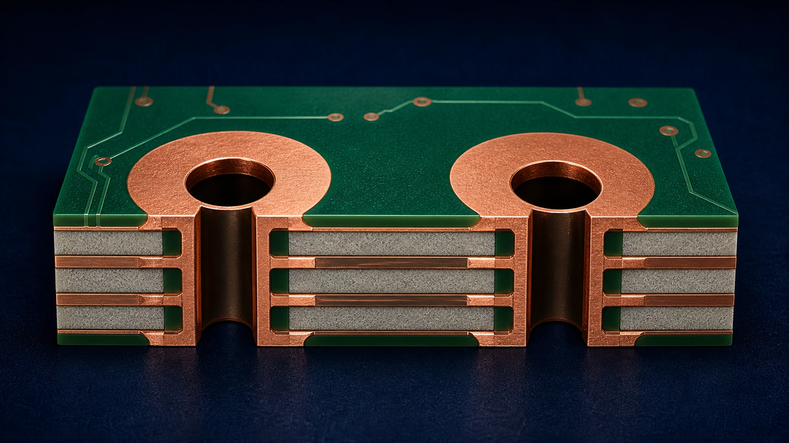
A pad is a copper land associated with a connection. When a hole passes through that land, the surrounding copper forms the annular ring. For a centered circular hole and pad, the ring appears uniform; an offset hole leaves a narrower region on one side.
The outer surface is only one view of this relationship. A plated through hole can connect to copper lands on internal layers, where alignment and remaining copper also matter. An acceptable-looking top pad does not establish that all internal connections have the required margin.
Identify whether the discussion concerns a nominal design allowance, a production-drill calculation or a finished-board acceptance measurement. These are related but not interchangeable. Ask the fabricator to state the basis used in its engineering review before comparing its result with a CAD rule.
Annular ring versus pad size and hole size
In ideal concentric circular geometry, radial ring width is half the difference between pad diameter and hole diameter. That relationship is useful for understanding the design, but the hole diameter used must match the purpose of the calculation.
A CAD view based on the smaller plated finished opening can overstate the copper margin that remained when the larger production hole was drilled. Actual pad etching and hole offset further change the narrowest remaining ring. A symmetric nominal allowance is therefore not a complete manufacturing analysis.
Increasing the pad can improve margin, but may reduce clearance to traces, planes or neighboring pads. Reducing the hole can also increase margin, but only if the finished opening remains suitable for electrical, plating and assembly requirements. Neither change should be made automatically to silence a rule violation.
For a noncircular pad or slot, inspect the local narrowest copper and the connection to the trace. A single equivalent diameter may hide the critical feature. Provide the actual geometry when requesting review.
Finished hole versus drill tool size
The finished size of a plated hole is the opening after the specified plating and finishing operations. The drill tool creates the production hole before that buildup. Fabricators select tool sizes and allowances to achieve the specified finished result using their process.
Do not use the finished opening alone to approve drill-to-pad margin. Confirm how the supplier interprets the drill file and which production diameter it uses for annular-ring checks. The PCB manufacturing tolerance guide explains the broader distinction between tool size, finished hole and dimensional acceptance.
Clearly distinguish plated and non-plated holes. A non-plated mounting hole may require copper clearance rather than an electrical connection to a barrel. A small component hole must not be treated as an adjustable via just because its diameter is small. Mark connector and press-fit requirements explicitly.
Drill wander and registration
Mechanical drilling can place the actual hole away from the intended center. Imaging and layer alignment can also place the copper land away from its nominal relationship to that hole. Multilayer fabrication combines these effects, so the result must be reviewed as a complete construction.
Drill wander and image misregistration are not the same fault. A hole pattern can be consistent with its drilling reference while an internal layer is displaced. Conversely, copper patterns can align while a drilling error reduces the local ring.
When investigating a problem, retain the hole identifier, affected layer and position within the board. Ask the supplier to compare the manufactured feature with the approved data and process references. A general statement that the drill is off center is insufficient to identify which operation needs attention.
Do not assume all positional variations can be added using an improvised rule. The fabricator should establish the relevant allowance for its process and construction; the customer should define the connection and acceptance requirements it must preserve.
Outer-layer versus inner-layer annular ring
Outer and inner layers experience different processing sequences. Inner copper is patterned before lamination, while outer patterning and plating follow the selected fabrication route. Material movement during lamination, drilling alignment and imaging can therefore affect their margins differently.
Review each connected internal land, not only the outer pad diameter in the footprint. Internal pad sizes or thermal connections can differ from the external land. Changes to nonfunctional pads also need review against the agreed construction and requirements.
Surface inspection cannot directly show every internal connection. Where required, agree the appropriate inspection or cross-section evidence with the fabricator. Do not specify a universal destructive-test frequency or assume a surface photograph proves internal compliance.
Annular ring and via reliability
The ring contributes copper connection margin between the hole region and the surrounding circuit. In a plated interconnect, the barrel and connected lands form part of the electrical and mechanical structure. Reduced margin may make that relationship less robust, particularly where local geometry is already constrained.
Ring width alone does not establish via reliability. Barrel plating, hole preparation, material expansion, board thickness and thermal exposure also matter. A large pad does not compensate for an unrelated barrel defect, and a passing continuity test does not by itself demonstrate long-term reliability.
Specify what evidence is needed for the product’s risk level and applicable requirements. Keep the detailed lifetime and thermal-cycling qualification with a dedicated via-reliability review rather than inferring it from one geometric dimension.
Annular ring in dense BGA designs
Dense BGA escape regions often place small pads, vias and traces close together. Increasing a via pad can block a routing channel; shrinking it can remove manufacturing margin. The decision should include the actual layer transitions and space available around neighboring connections.
Use the BGA fanout and escape-routing guide for routing architecture. Here, identify the vias with the least hole-to-pad margin and ask whether the proposed fabrication route supports them without unapproved geometry changes.
If conventional through vias cannot provide the required routing space and connection margin together, another interconnect structure may be considered. The PCB via types guide explains those options. Moving to microvias or another HDI structure is a construction change, not permission to reuse a through-hole annular-ring rule unchanged.
Annular ring and heavy copper
Thicker copper changes the etching challenge and the relationship between artwork and finished features. The pad boundary and nearby clearance must be manufacturable together. A design-rule set suitable for a lighter copper construction may not support the same geometry with heavier copper.
Review starting and finished copper assumptions, including differences between inner and outer layers. The PCB copper weight guide covers selection; the annular-ring question is whether the resulting land and surrounding pattern retain the required margin.
Do not equate thicker copper with automatically better ring geometry. Ask the fabricator whether pad enlargement, spacing changes or another construction is necessary. Approve changes against connectivity and routing constraints, rather than accepting a generic heavy-copper capability statement.
Common annular-ring problems
Drill breakout occurs when the hole reaches or passes the pad edge at a location. Whether a particular result is acceptable depends on the affected layer, connection and applicable specification. Avoid a blanket claim that every observed breakout has the same acceptance status.
Other problems include insufficient pad diameter, internal misregistration, use of finished-hole dimensions in a production-drill calculation, and routing that leaves no room for an adequate land. Fabrication notes can also conflict with the drill data or footprint.
Separate design margin from production conformity. If the approved design already lacks the required allowance, the release package needs engineering resolution. If the design is adequate but the manufactured board differs, the supplier needs a documented disposition. Do not approve an exception merely because the board still conducts during a quick test.
How to review annular ring before fabrication
- Verify the finished-hole requirement. Identify connector, press-fit and other holes whose opening cannot change without approval.
- Verify pad geometry. Check the relevant lands and trace connections on each layer, including the smallest local dimension.
- Identify plating status. Separate PTH, NPTH and via instructions so the supplier does not infer their purpose from size alone.
- Review the stackup. Confirm layer order, copper and interconnect construction used for the manufacturing assessment.
- Identify critical features. Mark dense BGA regions, tightly constrained component holes and internal connections.
- Check process capability. Obtain the supplier’s proposed drill basis, registration allowance and any required geometry adjustment.
- Confirm quality requirements. Agree the applicable standard, revision, class and customer-specific conditions.
- Resolve conflicts before release. Approve one controlled data set and record exceptions with their scope and decision owner.
The IPC Class 2 versus Class 3 guide explains the role of product requirements. A class label alone should not replace the applicable specification or be treated as a universal ring dimension.
Annular-ring checklist
- Through vias: confirm the drill basis, connected layers and permitted hole adjustments.
- Component holes: preserve insertion fit, pad geometry and soldering needs.
- Press-fit holes: provide the connector application specification and required finished-hole construction.
- Internal layers: review connected lands and how their alignment will be verified.
- High-density areas: resolve the trade-off between routing clearance and connection margin before layout release.
- Fabrication drawing: identify requirements, revisions and any approval needed for data-preparation changes.
Use the checklist to record a decision, not simply a checked box. A useful review entry identifies the feature, concern, supplier response and approved outcome. That record helps a later revision retain the reason for a larger pad or restricted drill change.
Information required from the customer
Provide Gerber or ODB++ data, drill files, fabrication drawing, finished-hole sizes, stackup, copper requirements and via definitions from the same revision. Include the applicable IPC or customer specification, class and revision where required, plus connector and press-fit documentation.
Identify which holes may be adjusted and which are fixed by the product interface. Mark critical internal connections or dense areas and state the inspection evidence expected at delivery. This lets the fabricator assess actual manufacturing margin instead of guessing the purpose of each feature.
Review hole-to-pad geometry before fabrication
Excel Circuit provides in-house PCB design engineering and coordinates qualified PCB manufacturing resources alongside sourcing, in-house SMT assembly and turnkey PCBA. Its PCB manufacturing coordination services can help align hole and land requirements with the proposed construction.
Send your Gerber data, drill files and finished-hole requirements if you need annular-ring and drill-to-pad relationships reviewed before fabrication. Submit your annular-ring review inputs.