Controlled impedance PCB manufacturing depends on both the design and the actual fabricated geometry and material properties. A nominal target can shift with trace width, copper thickness, dielectric thickness, Dk, etching, plating and stackup variation. The design data, approved stackup and fabrication process therefore need coordinated requirements, followed by an agreed verification method.
A target value alone is not a complete order instruction. Define the relevant structures, allowable tolerance, permitted adjustments, coupon strategy and test-report expectations before fabrication. Impedance-aware routing and a production impedance report answer different questions.
| Stage | What is controlled | Why it matters | Release evidence |
|---|---|---|---|
| Stackup definition | Dielectric and copper structure | Establishes the physical transmission line | Approved layer and construction record |
| Trace geometry | Width, spacing and reference relationship | Influences the intended impedance | Identified structures and layers |
| Material properties | Relevant Dk, Df and construction | Affects impedance and dielectric loss | Approved material basis |
| Fabrication compensation | Process-dependent artwork adjustments | Targets the required finished geometry | Approved adjustment scope |
| Coupon creation | Representative test structures | Enables production measurement | Coupon-to-board mapping |
| TDR test | Measured impedance response | Compares production with specification | Agreed test record |
| Reporting | Results, limits and traceability | Supports customer acceptance | Identified lot, coupon and result |
What is controlled impedance PCB manufacturing?
Impedance-aware design selects an appropriate structure and routing for the circuit. Controlled-impedance fabrication translates the approved design into material and geometry controls. Impedance verification measures defined structures and compares the results with the agreed limits.
These activities should connect through one specification. A designer’s field-solver result is not a measurement of the manufactured panel, and a coupon pass does not independently validate the entire channel. The customer and supplier must agree what the production test demonstrates.
For design-side topology and timing considerations, see the DDR routing and signal-integrity guide. This article focuses on the fabrication handoff, acceptance and documentation rather than choosing interface targets or teaching transmission-line theory.
Why fabrication changes impedance
Fabrication changes the physical conductor and dielectric structure from the idealized design model. Etching influences conductor width and sidewall shape. Plating can affect outer-layer copper thickness, while lamination and resin distribution influence dielectric spacing.
Material variation and construction details can change the dielectric behavior used by the model. Copper roughness also becomes relevant to loss and modeling accuracy in some high-frequency applications, but it should not be presented as the dominant variable in every board.
Ask the fabricator which dimensions and material assumptions it will use for the proposed stackup. If the customer’s model uses a different copper profile, dielectric thickness or Dk basis, reconcile that difference before deciding that the design and fabrication calculations agree.
The PCB manufacturing tolerance guide explains general dimensional variation. For controlled impedance, the concern is how those variables combine to affect the specified electrical result, not whether each nominal dimension appears individually reasonable.
Stackup definition
The manufacturer needs a clear layer order, reference-plane arrangement, dielectric thickness, copper requirements, material family and impedance targets. A total board thickness without the internal construction is insufficient to define a controlled transmission line.
Separate customer-fixed requirements from supplier-proposed details. If the fabricator may select prepreg constructions or adjust dielectric spacing, identify the approval process and any mechanical limits. The PCB stackup design guide covers layer planning; the manufacturing handoff must preserve the approved result.
Include the stackup revision in the production package. A coupon designed for an earlier layer spacing is not representative merely because the board name is unchanged. Resolve substitutions and construction changes before manufacturing and measurement records are generated.
Single-ended versus differential impedance
A single-ended impedance requirement describes a signal conductor relative to its reference structure. A differential requirement describes the pair under differential excitation and depends on the relationship between both conductors and their references.
For production review, identify the trace type, layer, reference layers and relevant geometry. A differential pair requires an explicit pair structure, including spacing; it should not be inferred from two nearby single-ended traces. Do not assume that a differential target is always exactly twice a separate single-ended value.
Use consistent structure names across the drawing, stackup proposal, coupon and report. This simple mapping helps prevent a correctly measured coupon from being assigned to the wrong requirement.
Impedance tolerance
Impedance tolerance defines the allowable production range around the specified target. It gives the supplier an acceptance requirement and gives the customer a basis for interpreting test results. There is no universal percentage that is suitable for every interface and construction.
The design owner should establish the required range from the application, then obtain supplier confirmation that the construction and measurement plan can support it. An unnecessarily tight range can reduce process margin or require additional control without improving the product’s useful performance.
Specify whether limits are absolute values or a percentage of the target, and which test result is compared with them. Agree the evaluation region and result convention rather than assuming every supplier reports the same statistic. Measurement uncertainty and method differences should be addressed when they are significant to the requested acceptance range.
Etch compensation
Etch compensation adjusts manufacturing artwork to account for the process and obtain the intended finished copper geometry. Design width, production artwork width and finished width may therefore differ.
Distinguish routine process compensation from an engineering change to the approved electrical structure. A proposed change to nominal line width, pair spacing or dielectric thickness may require design approval even when intended to improve impedance. The fabricator should identify the proposed change and its effect on other clearances or constraints.
Do not apply independent compensation in both CAD and fabrication without coordination. Supply the intended design geometry and let the agreed workflow identify who controls production adjustments. No proprietary formula or universal correction value is necessary to document that responsibility.
Impedance test coupons
An impedance coupon is a test structure manufactured to represent specified transmission-line construction on the board. It can provide accessible test connections without requiring the production circuit itself to accommodate the measurement setup.
Representation must be established deliberately. Match the relevant layer, reference arrangement, dielectric construction, copper and line or pair geometry. Consider mask coverage and other structural details when they affect the modeled line. A generic coupon carrying the right target label is not sufficient evidence.
Coupon placement on a fabrication panel and the number of coupons or measurements depend on the production and verification plan. Agree coverage and traceability with the supplier instead of prescribing a universal layout or assuming one coupon proves every location on every board.
Identify who designs the coupon and who approves its relationship to the customer requirement. Changes to the board construction should trigger review of the associated coupon definition.
TDR testing
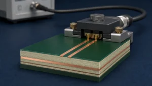
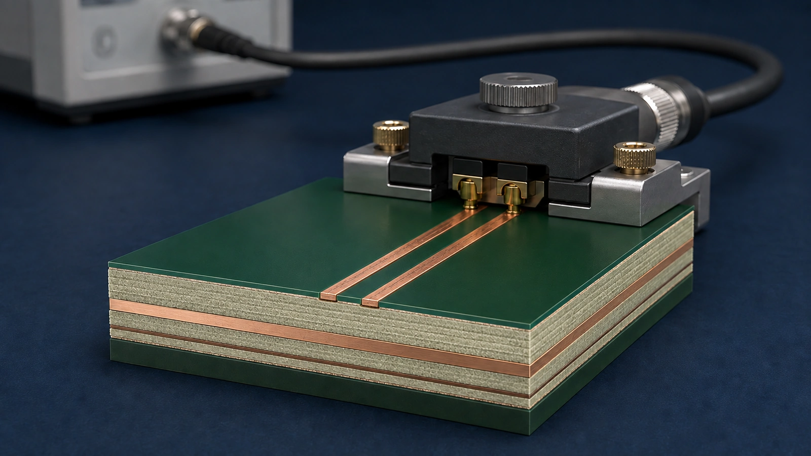
Time-domain reflectometry, or TDR, applies a fast electrical transition and observes reflections associated with impedance changes. The resulting profile is used to evaluate the specified structure over an agreed measurement region.
The launch, probe and connection can introduce responses that are distinct from the transmission line being evaluated. Measurement setup, calibration and interpretation therefore matter. The supplier should use an appropriate controlled procedure, with the relevant test conditions available when required for acceptance.
Compare the reported result with the specified target and limits. If a profile is outside limits or ambiguous, investigate the structure, setup and production record before accepting a revised measurement. A selected passing point should not replace the agreed evaluation method.
TDR does not prove all high-speed performance. A passing impedance coupon does not establish channel insertion loss, crosstalk, timing, connector performance or system compliance. Those need the appropriate design analysis and product verification.
Controlled impedance reporting
A useful report connects a measured result to the requirement and production material it represents. Suppliers differ in report format and standard deliverables, so confirm the required information before placing the order.
- Requirement: target, tolerance, structure name and relevant layer.
- Test identity: coupon identifier and applicable test record or profile.
- Result: measured value or evaluation result under the agreed convention, with pass/fail status.
- Traceability: board revision, stackup revision and production lot or panel reference as required.
- Exceptions: approved deviations, retest rationale or unresolved discrepancies where applicable.
A generic certificate saying impedance controlled may not satisfy a requirement for individual readings or trace plots. Conversely, a lengthy plot collection without coupon-to-structure mapping may be difficult to use. Specify the evidence needed for incoming acceptance and future traceability.
Controlled impedance and material selection
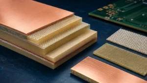
Material selection affects the dielectric properties and available construction used to achieve the target. Dk influences impedance and propagation, while Df contributes to dielectric loss. Thickness consistency and the selected resin/glass construction also matter.
Use a material-property basis appropriate to the frequency, construction and modeling method. A nominal datasheet Dk is not an immutable value that applies to every thickness or test method. The PCB material selection guide explains how to interpret Tg, Td, CTE and Dk/Df.
Do not approve a replacement laminate on Tg alone. If the substitution changes electrical properties or available dielectric construction, review both the design model and the production test plan. Passing an impedance target still does not prove that a changed material meets the channel loss budget.
Common controlled-impedance problems
Missing targets or tolerances leave the supplier without an acceptance basis. Ambiguous layer names, conflicting drawings and an outdated stackup can lead to a valid test of the wrong structure. Unreviewed material substitutions can invalidate the assumptions used for the original model.
Insufficient coupon definition makes it unclear what the measurement represents. Overly tight limits without an application need can create avoidable production difficulty. Treat these as release-package problems to resolve before fabrication rather than issues to negotiate after boards arrive.
Assign an engineering decision owner for each unresolved item. The purchasing specification should reference the approved answer, not merely the latest email attachment. This keeps quotation, fabrication and incoming inspection aligned.
What to put on the fabrication drawing
Useful controlled-impedance notes identify the target, allowable tolerance, layer, trace type and stackup requirement. They also state the required test and report deliverables and any restrictions on geometry or material changes.
There is no single mandatory drawing format for every project. A structure table can work well when several layers or line types are controlled, provided its labels match the manufacturing proposal and coupon record. Keep net-specific restrictions clear where only selected geometry may be adjusted.
Ask the supplier to return an approved construction and identify exceptions before release. The drawing should distinguish a requirement from an illustrative design assumption so that an example is not mistaken for a fixed manufacturing instruction.
Controlled impedance review checklist
- Target: identify each required impedance structure.
- Tolerance: state the allowable range and evaluation basis.
- Layer: identify signal and reference layers consistently.
- Geometry: confirm widths, pair spacing and permitted changes.
- Material: approve the property basis and substitution controls.
- Stackup: release a controlled construction revision.
- Coupon: confirm representative structures and traceability.
- Test: agree the method, coverage and response to exceptions.
- Reporting: specify readings, profiles and lot references as needed.
Information required from the customer
Provide Gerber or ODB++ data, fabrication drawing, stackup, impedance targets and allowed tolerances. Identify relevant nets or layers, material requirements, copper and any geometry that cannot change. Include the TDR and report requirements expected at delivery.
Where an interface has a separate loss or performance requirement, state it explicitly. Ask which requirements are verified by the proposed coupon measurement and which require additional product-level evidence. That prevents a fabrication report from being used beyond its intended scope.
Review manufacturing and verification requirements
Excel Circuit combines in-house PCB design engineering with qualified PCB manufacturing resources, component sourcing and in-house SMT assembly. Its PCB manufacturing coordination services can help align the proposed construction and supplier verification with the customer’s release requirements.
Send your stackup, impedance targets and fabrication data if you need the controlled-impedance requirements reviewed before PCB fabrication. Submit your controlled-impedance review inputs.