Contents
DDR PCB routing is difficult because the layout must preserve timing relationships among DQ/DQS byte lanes, address/command/control signals and clock while also controlling topology, impedance, return paths, crosstalk, package breakout and stackup transitions. It is not a task of making every trace the same physical length. Constraints must come from the selected DDR generation, controller and memory documentation, package delays, board construction and validated timing architecture.
DDR Rules Must Be Generation- and Controller-Specific
DDR3, DDR4, DDR5 and LPDDR families do not share one universal routing recipe. Signal functions, topology, termination, training behavior and timing relationships can differ by generation, controller, memory device, rank arrangement and package. Begin with the controller design guide and memory documentation for the exact components, then translate those requirements into named CAD constraint groups.
Reference designs can show a proven architecture, but their widths, lengths, spacing and via structures belong to their stackup and package implementation. Reuse the reasoning only after recalculating the physical constraints for the actual board. Avoid mixing a DDR4 fly-by assumption or matching rule into a DDR5 or LPDDR design without device-specific confirmation.
Plan Memory Placement Before Detailed Routing
DDR memory placement should organize the controller or FPGA, memory packages, termination and decoupling so byte lanes, clock and address/command routes have direct corridors, coherent breakout directions and continuous references. Poor orientation can force excessive tuning, extra vias, layer changes and congestion. Place from the required topology and package pin fields outward rather than positioning components first and trying to repair the timing architecture with serpentine routing.
Review controller and memory pin maps, BGA escape channels, available routing layers and mechanical keepouts together. Preserve room for power/ground access and local decoupling paths. The existing FPGA and embedded board engineering example shows how package, power and routing constraints interact at system level.
Separate DDR Signal Groups and Their Timing Relationships
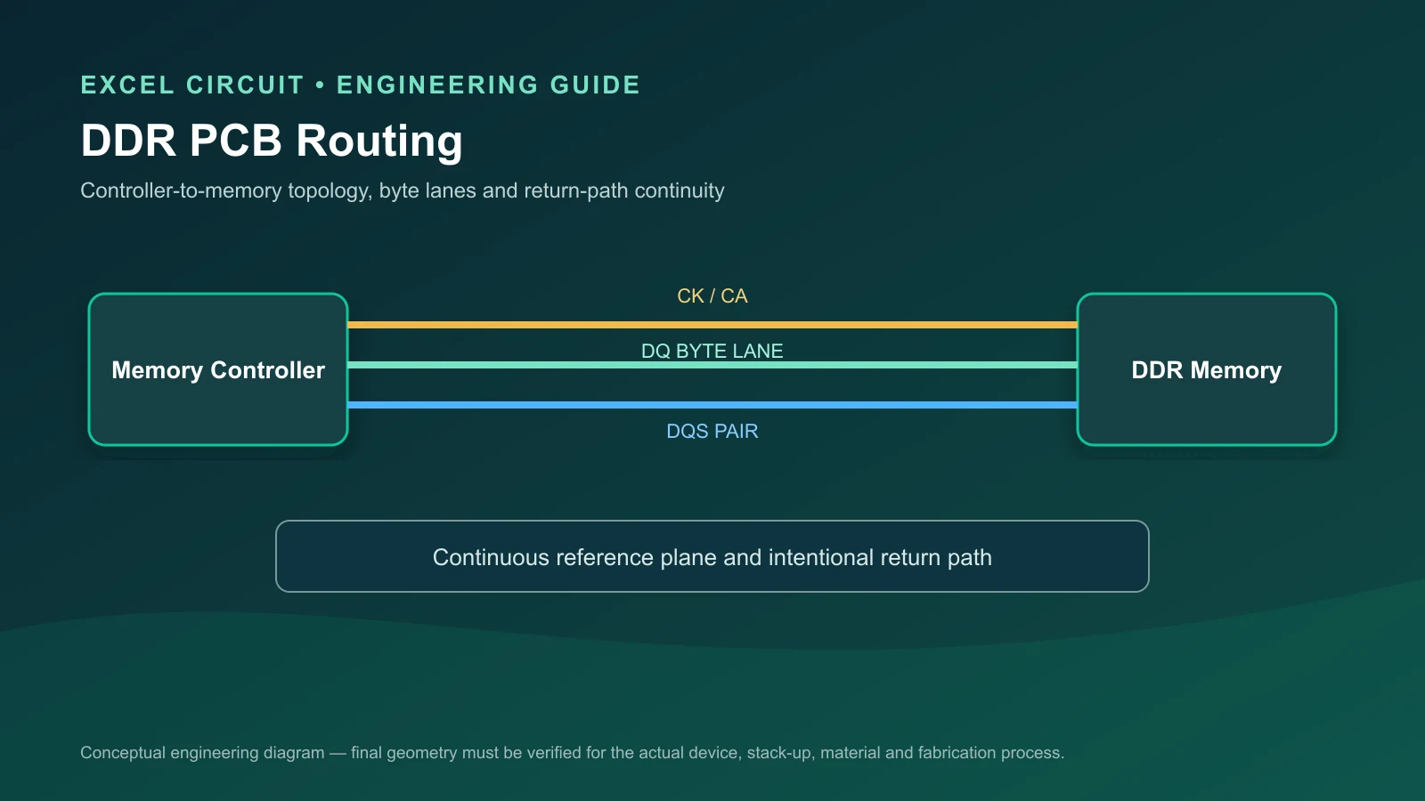
Constraint classes should reflect functional relationships instead of one bus-wide length target. Common groups include DQ data, differential DQS strobes, DM or DBI where the selected interface uses them, address/command/control, differential clock where applicable, and reset or lower-speed controls. Each group may have different topology, timing, termination and reference requirements.
DQ and DQS Byte Lanes
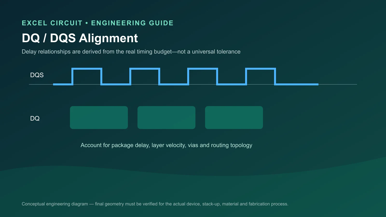
DQ signals should be constrained relative to their associated DQS strobe within the correct byte lane, using the controller’s timing model and package information rather than a universal skew number. Keep the lane physically coherent, use consistent routing structures where practical, and account for propagation and transition differences. Do not match unrelated byte lanes or the complete DDR interface to one arbitrary physical length.
DQS/DQS# pair quality, DQ grouping, DM/DBI association and lane mapping depend on the memory architecture. Package delay may consume part of the timing budget even when PCB lengths appear equal. Where tools permit, manage electrical delay rather than only geometric length and verify that constraints remain assigned after pin swaps or routing-layer changes.
Address, Command, Control and Clock
Address/command/control nets may use a topology and load sequence different from the DQ/DQS point-to-point or byte-lane relationships. Clock routing may be differential where defined by the interface and should maintain controlled geometry, reference continuity, suitable pair symmetry and controlled transitions. Exact matching and termination must follow the controller architecture, not a generic DDR checklist.
Choose DDR Topology From the Actual Architecture
DDR topology matters because it determines branch behavior, load order, reflections, termination placement and the timing seen by each memory device. Point-to-point, fly-by, historical T-style and other multi-load arrangements solve different architectural problems. The appropriate choice depends on DDR generation, controller support, device count, package arrangement and termination strategy; no topology is universally best for every DDR interface.
Fly-by routing is associated with particular address/command/clock architectures, while data lanes commonly have different relationships. Branches and stubs should be evaluated as transmission-line structures. On-die, series, parallel or other termination approaches are controller-, memory- and topology-dependent; this guide does not prescribe resistor values or assume the same method applies across generations.
Length Matching Means Controlling Propagation Delay
All DDR traces do not need equal length; matching controls specified propagation-delay relationships within functional groups and against the interface timing budget. Electrical delay depends on routing layer, dielectric environment, geometry, vias and package contribution as well as physical length. Assign DQ-to-DQS, clock and address/command constraints separately using the controller design guide, memory data, package delays where available and timing or SI analysis.
Shorter routing can reduce loss and exposure, but “shortest possible” is not an independent goal if it breaks topology, reference continuity or group relationships. Do not tune every net to the longest accidental route. Improve placement and route architecture first, then add only the delay required by the verified constraints.
Use Serpentine Tuning Carefully
Dense meanders can couple to themselves and adjacent nets, consume routing space, add loss and create local discontinuities. Spread tuning where geometry and coupling analysis support it and avoid tight accordion patterns used only to make a length report look uniform. Tuning quality is judged by resulting delay and channel behavior, not by visual symmetry.
Build DDR Constraints From the Approved Stackup
PCB stackup affects DDR routing by defining controlled-impedance geometry, propagation velocity, adjacent reference planes, routing-layer capacity, BGA escape options and the electrical behavior of via transitions. A length on one layer may not produce the same delay on another. Define trace and spacing rules from the approved dielectric and finished-copper construction, then keep routing and analysis synchronized with that stackup revision.
The PCB Stackup Design Guide explains materials, reference layers and fabricator coordination in detail. For DDR, identify the routing and reference layer for every group, ensure controlled geometry is manufacturable, and review whether layer changes create delay or return-path differences that need to be included in the constraint model.
Controlled Impedance Is a Construction, Not a Width
DDR transmission environments depend on trace geometry, reference location, dielectric thickness and properties, finished copper and fabrication tolerance. A generic trace width or single impedance number cannot be applied to every DDR interface. Targets and tolerances must come from the controller and memory requirements, then be converted into per-layer geometry with the selected fabricator.
Protect DDR Return-Path Continuity
Return-path continuity matters in DDR because fast signal edges contain high-frequency energy whose return current follows a low-impedance path near the signal’s reference structure. Plane gaps, voids or unsupported reference changes can enlarge the loop, disturb impedance and increase coupling or EMI. Route critical nets over continuous references and review package breakout, connector regions and every layer transition as complete signal-return structures.
When a DDR route changes layers and reference structures, a nearby return connection may be needed to support the transition. The correct stitching or decoupling structure depends on the two references, their net relationship and the stackup. Avoid blanket “never cross any split” wording, but treat a discontinuity under a critical DDR route as a design risk requiring explicit analysis.
Control Vias and BGA Breakout
Vias affect DDR signals through inductance, capacitance, impedance discontinuity, unused stub, reference-path interruption and transition asymmetry—not simply by adding physical length. Vias are not forbidden, but unnecessary or inconsistent transitions consume channel and timing margin. Review pad, antipad, barrel, stub and return support against the data rate, layer assignment, board thickness and fabricator capability.
BGA fanout determines which layers and channels each byte lane can reach. Dense inner rows, antipad fields and power/ground breakout can fragment routing capacity before DDR tuning begins. Use the BGA fanout and escape routing guide to evaluate dog-bone, via-in-pad, through-via or HDI options without assuming one method from package pitch alone.
Reduce Crosstalk Without Universal Spacing Rules
DDR crosstalk is reduced by controlling spacing, parallel exposure, reference-plane proximity, routing-layer arrangement and aggressor/victim relationships according to edge rate and stackup. Separate sensitive groups from clocks and switching nodes, avoid long close parallel runs and inspect dense escape and tuning regions. A fixed “3W” multiplier is only a heuristic; stackup-specific coupling analysis should define spacing where margin is important.
Serpentine segments deserve particular attention because adjacent turns and neighboring routes may couple over substantial length. Crosstalk review should include package breakout and layer transitions, not just open routing fields. Pair visual inspection with constraint checks or SI analysis when the architecture has limited noise or timing margin.
Coordinate DDR Power Integrity and Decoupling
DDR behavior depends on memory and controller rails, references, termination supplies where applicable, ground connectivity and simultaneous switching response. A timing-correct route can still fail if PDN impedance, rail noise or reference disturbance reduces the receiver margin. Review regulator path, planes or pours, via arrays, package access and transient current as one network. The broader FPGA power integrity and decoupling guide explains how those PDN paths are planned for programmable-logic loads.
Decoupling effectiveness depends on component requirements, capacitor frequency behavior, placement, mounting inductance, via geometry and power/ground access. Do not apply universal capacitor values or distance rules. Coordinate the memory package breakout with decoupling connections before routing channels are consumed, and use SI/PI analysis where it can change stackup, placement, routing or PDN decisions.
Simulation, Fabricator Coordination and Release Verification
SI simulation can compare topology, termination, reflections, eye behavior, timing margin, crosstalk and via discontinuities where adequate package and interconnect models are available. The required depth depends on interface risk; every DDR board does not need an identical workflow. Document assumptions and convert results into constraints rather than presenting plots as proof by themselves.
Align the released layout with qualified PCB manufacturing resources by confirming stackup, impedance construction, trace/space, materials, via structures and layer count with the selected fabricator. Excel Circuit provides fabricator coordination through qualified PCB manufacturing resources. Ensure the final PCB rules, stackup drawing, impedance notes and drill/via table describe the same revision.
Common DDR Routing Mistakes
- Matching every signal to one arbitrary length instead of group timing relationships.
- Placing memory without proving topology, escape and routing corridors.
- Using excessive serpentine tuning to compensate for weak placement.
- Crossing reference discontinuities without reviewing the return-current detour.
- Using excessive or asymmetric via transitions within related routes.
- Mixing DQ byte lanes or losing DQ/DQS group assignments.
- Ignoring BGA antipads, inner-row escape and power/ground access.
- Copying impedance geometry from another stackup or reference design.
- Applying DDR3/DDR4 assumptions directly to DDR5 or LPDDR.
- Completing route tuning before power and decoupling paths are validated.
| DDR signal group | Main routing concern | Verification focus |
|---|---|---|
| DQ with DQS/DQS# | Byte-lane timing and consistent transition structure | DQ-to-DQS delay, package effects and lane assignment |
| DM/DBI where applicable | Association with the correct byte lane | Controller-specific group constraints |
| Address/command/control | Topology, load order, branching and termination | Generation/controller design-guide compliance |
| Clock | Differential geometry, reference and transitions | Pair quality, topology, impedance and timing |
| Reset/other controls | Function-specific timing and noise exposure | Device requirements rather than bus-wide matching |
DDR PCB Layout Review Checklist
Before DDR layout release, confirm the exact memory generation and devices, controller design guide, topology, placement, byte-lane mapping, stackup, impedance construction, group-specific timing constraints, continuous references, via transitions, crosstalk, termination, memory rails and decoupling. Complete DRC and review SI/timing where project margin requires it, then verify that the fabrication drawing, stackup, constraints and released PCB database use the same revision.
- Controller, memory devices, ranks, bus width and generation confirmed.
- Placement and BGA escape support the chosen topology.
- DQ/DQS byte lanes and other signal groups identified.
- Approved stackup and per-layer impedance rules loaded.
- Electrical-delay constraints assigned by functional relationship.
- Package delays included where reliable data is available.
- Reference planes and return transitions reviewed.
- Via and test-point stubs assessed.
- Crosstalk checked in escape, parallel and tuning regions.
- Termination follows the controller/memory architecture.
- Power, reference rails and decoupling paths reviewed.
- DRC, SI/timing and fabrication review completed as required.
Engineering Context for Complex DDR Boards
For projects requiring external support, Excel Circuit’s high-speed PCB design and Embedded & FPGA PCB Design teams coordinate placement, stackup, constraints, BGA breakout, SI/PI and DFM. The Embedded & FPGA PCB Design Guide provides the broader architecture, power-sequencing and bring-up context.
FAQ
What length-matching tolerance should be used?
There is no universal value. It depends on DDR generation, devices, topology, package delays, data rate, stack-up, and timing margin. Derive it from device documentation and timing or SI analysis.
Should all DDR signals have the same length?
No. Constraints follow functional groups. DQ relates to its DQS; command/address/control and clock use different requirements.
Can a reference design trace width be reused?
Only after recalculation for the actual stack-up and confirmation by the fabricator. Width alone does not define impedance.
When is simulation justified?
Use it when margin is limited, channels are long, transitions are numerous, packages are dense, or stack-up constraints are unusual. Simulation should inform topology, termination, geometry, and rules.
Request a DDR PCB Engineering Review
If you are reviewing a DDR-based PCB, share the schematic, processor/FPGA package, memory devices, stackup, routing constraints and manufacturing requirements for engineering review.