
PCB manufacturing tolerances describe the permitted variation between design dimensions and the finished board. Fabrication is not dimensionally perfect: conductor width, drilled holes, finished hole size, routed dimensions, board thickness and layer registration all vary. A production drawing should distinguish critical dimensions, nominal dimensions and supplier-controlled dimensions instead of applying unnecessarily tight limits everywhere.
The useful question is which variation could prevent the board from fitting, connecting or working. Actual limits depend on material, layer count, copper weight, board dimensions, hole size and aspect ratio, plating, routing, panelization and the agreed specification. Confirm critical requirements for the actual construction before release; a generic capability list cannot establish acceptance for every board.
| Feature | Why it varies | Why it matters | Specify carefully when |
|---|---|---|---|
| Trace width / spacing | Etching and copper thickness | Electrical geometry and separation | Routing is dense or impedance controlled |
| Drill location | Drilling and layer registration | Hole-to-pad alignment and fit | Hole patterns locate connectors or hardware |
| Finished hole size | Tool selection and plating | Pin insertion and press-fit compatibility | A component specifies a finished-hole range |
| Board outline | Routing or scoring and separation | Enclosure and mating-feature fit | Edges, slots or cutouts locate the board |
| Board thickness | Material, copper and lamination | Connector engagement and mechanical fit | Card-edge, press-fit or stackup needs control |
| Layer registration | Imaging, material movement and lamination | Hole-to-copper and multilayer alignment | Dense interconnects leave little process margin |
What PCB manufacturing tolerance means
A nominal dimension is the intended size. A tolerance defines the acceptable range around that size, which need not be symmetric. Manufacturing variation is the spread produced by the process. Process capability describes how that process performs against specified limits under defined conditions; it is not another name for the tolerance printed on a drawing.
A minimum manufacturable feature and a dimensional tolerance answer different questions. The first concerns whether a feature can be produced reliably; the second concerns acceptable variation in its result. Passing a minimum trace-width check does not prove that a tightly controlled conductor will meet an electrical requirement.
Tighter limits reduce the margin available for normal variation. Before adding them, identify the failure they prevent and how the finished feature will be measured. For supplier-controlled dimensions, reference an agreed specification or approved construction rather than leaving acceptance implicit.
Trace width and spacing tolerance
Etching changes the relationship between artwork and finished copper. Copper thickness, feature density and processing affect the resulting conductor profile and isolation gap. Inner and outer layers can follow different processing sequences, particularly where outer-layer plating contributes to finished copper.
For dense routing, inspect the narrowest conductors and gaps alongside neighboring copper. Heavy copper changes the etching challenge, so a layout rule suitable for a lighter construction should not automatically carry over. The PCB copper weight guide covers copper-selection trade-offs; here the decision is whether the resulting geometry needs explicit control.
Give the fabricator the intended finished copper and critical electrical requirements. Ask what artwork compensation is needed and which customer geometry must remain unchanged. Do not independently compensate the same feature in CAD and manufacturing without agreement. If width is an acceptance dimension, define the layer and measurement convention because the etched cross-section is not necessarily rectangular.
Drill diameter and finished hole size
Drill tool size is the cutting-tool diameter used during manufacture. Finished plated through-hole size describes the opening after the specified plating and finishing processes. The tool is normally selected with allowances for the process; it should not be substituted directly for the finished-hole requirement.
A non-plated hole has no intentionally plated barrel, but its finished size still depends on drilling or routing and the agreed acceptance conditions. Separate PTH and NPTH requirements clearly in drill data and the fabrication drawing. Identify plated slots as such rather than relying on their shape to communicate intent.
Connector pins need adequate fit across pin and hole variation. Press-fit systems can also constrain hole-wall construction and finished-hole range. Provide the connector manufacturer’s current application requirements and ask the fabricator to confirm compatibility. A generic clearance-hole note is insufficient evidence for a compliant press-fit interface.
For a critical hole, record its identifier, finished size limits, plating status and functional purpose. Agree whether inspection occurs before or after final finish and how results will be reported. Purchasing should quote against that requirement rather than a nominal drill diameter alone.
Drill position and hole registration
Drill position controls where the hole lies relative to its intended reference. A hole can meet its diameter requirement while failing its location requirement. Connector patterns, locating pins and mounting hardware therefore require review of both size and position.
On a multilayer board, hole-to-pad alignment also depends on copper-layer registration. Annular ring is the copper remaining around a hole; it provides useful context for the alignment margin but is not a substitute for a complete hole-location specification. Dense designs need enough margin across the relevant layers, not just an acceptable appearance on the outer surface.
Identify the reference features used to locate a critical pattern. Ask the fabricator to review the whole relationship, including drill alignment and layer registration, rather than tightening individual coordinates without examining the intended fit.
Board outline and routing tolerance
The finished outline determines whether a PCB fits its enclosure and aligns with adjoining parts. CNC routing produces external edges, slots and cutouts, but tool geometry limits internal corner shape. A nominal square corner on a drawing does not by itself define a manufacturable internal corner.
Dimension the interfaces that actually locate the board: connector-to-edge relationships, mounting-hole locations, slot widths and seating surfaces. Supply the mechanical drawing with an unambiguous outline layer. Resolve differences between these files before fabrication rather than expecting the supplier to choose the correct version.
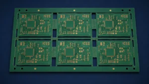
Define acceptance after the intended separation and cleanup operation. A breakaway remnant may matter even when the routed outline is correct. The PCB panelization and breakaway guide addresses method selection; this drawing should state which finished edges must meet the mechanical envelope.
Board thickness tolerance
Finished board thickness results from laminate cores, prepreg, copper and lamination. Material thickness and resin flow contribute to variation, so a nominal stackup total is not an exact prediction of every finished board. Do not apply a universal percentage to all constructions.
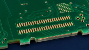
Card-edge connectors can require a defined mating thickness. Mechanical clamps and enclosures may constrain the total envelope, while press-fit systems can specify board and hole requirements together. State whether the thickness requirement includes copper, mask or other surface layers at the location being evaluated.
For impedance-controlled boards, the relevant dielectric spacing may need attention independently of overall thickness. Ask the fabricator to reconcile the approved stackup, electrical requirement and mechanical limit. Tightening the total thickness alone does not necessarily control the dielectric layer that determines a particular transmission line.
Layer-to-layer registration
Layer registration describes alignment between the copper patterns in a multilayer construction. Imaging, material movement during processing, lamination and subsequent drilling all influence the final relationship. A design that looks aligned in CAD must still allow for these manufacturing effects.
Dense interconnect regions and small capture features reduce available margin. Review the proposed stackup and interconnect structure before treating each layer as an independent two-dimensional drawing. Ask which alignment relationships are critical to the process and whether the intended construction is supported without changing electrical connectivity.
Keep the release decision focused on manufacturability of the complete structure. Detailed annular-ring sizing or HDI stackup design needs its own review; a general registration note cannot validate either.
Controlled impedance and dimensional variation
Impedance depends on trace geometry, copper thickness, dielectric thickness, dielectric properties including Dk, and the reference-plane arrangement. Etching affects the conductor shape. These variables interact, so a narrow trace-width tolerance alone cannot establish impedance compliance.
Provide the target impedance, applicable nets or layers, approved stackup assumptions and required verification. Clarify whether the fabricator may adjust conductor geometry and how proposed changes receive approval. If both geometry and impedance are independently constrained, confirm that the combination is feasible before ordering.
The useful output is an agreed construction and verification plan. Detailed field-solver methods and controlled-impedance manufacturing belong in dedicated guidance, rather than being inferred from a general tolerance table.
Why tighter tolerances can increase cost
Tighter tolerances may require additional process review, measurement, sorting or special controls. They can reduce usable process margin and affect yield. The commercial effect depends on the feature and construction; there is no defensible universal cost premium.
Ask the supplier to identify which requirements depart from its proposed normal process and explain the resulting controls. Compare alternatives by functional acceptability, inspection evidence and sourcing flexibility. Relaxing a nonfunctional cosmetic dimension may help, while relaxing a connector interface without engineering approval may create a more expensive assembly problem.
When should a dimension be tightly controlled?
Control a dimension tightly when its variation can violate a defined functional requirement. Start with the mating part or electrical need, then allocate an appropriate allowance to the PCB. Include the variation of adjoining parts instead of giving the board the entire available clearance.
- Electrical function: identify sensitive geometry and the performance it supports.
- Mechanical fit: identify locating surfaces, hole patterns and enclosure constraints.
- Connector compatibility: use the component application specification for holes and mating thickness.
- Safety: preserve required separation under the applicable product requirements; do not treat nominal CAD spacing as proof.
- Assembly and interchangeability: confirm the range that permits insertion, fixtures and replacement across production lots.
The broader DFM, DFA and DFT review framework helps assign these concerns to fabrication, assembly and test. This tolerance review converts the relevant concerns into measurable requirements.
Common tolerance specification mistakes
An unnecessarily tight global note can constrain every feature, including those with no functional need. Prefer explicit critical callouts and an agreed general rule. Conversely, a drawing containing only nominal dimensions can omit the requirement that matters most.
Other frequent ambiguities include PTH versus NPTH, tool size versus finished hole, unspecified thickness measurement conditions and conflicts between Gerber data and the drawing. Overconstrained dimension chains can also create mutually incompatible acceptance limits.
Resolve these issues in one controlled revision. Record approved exceptions rather than distributing them across informal messages. A successful sample does not establish the intended tolerance range unless the production requirement is documented.
PCB tolerance review checklist
- Conductors: identify critical widths, gaps, layers and finished copper assumptions.
- Holes: distinguish tool information from finished PTH, NPTH and plated-slot requirements.
- Outline: confirm edges, slots, cutouts and post-separation acceptance.
- Thickness: define finished condition, relevant location and mating-part needs.
- Stackup: reconcile material, copper, dielectric spacing and registration.
- Mechanical features: identify references and interface drawings.
- Impedance: agree targets, permitted adjustments and verification evidence.
- Critical dimensions: identify who approves limits and supplier exceptions.
Information required from the customer
Send Gerber or ODB++ data, drill files, fabrication drawing and stackup from the same revision. Include finished thickness and copper requirements, critical mechanical dimensions, finished-hole limits, impedance requirements and applicable drawing tolerances. Provide connector or enclosure information where it defines acceptance.
Mark critical features clearly and identify which nominal dimensions may remain supplier-controlled under an agreed specification. The PCB production-package checklist covers file completeness; the additional requirement here is clarity about the dimensional result those files must produce.
Review critical tolerances before fabrication
Excel Circuit combines in-house PCB design engineering with qualified PCB manufacturing resources and production-readiness support. Its PCB manufacturing coordination services help align design intent with the proposed fabrication route. Project-specific tolerances require confirmation for that construction.
Send your Gerber data, drill files, fabrication drawing and stackup if you need critical PCB tolerances reviewed before fabrication. Submit your PCB tolerance review inputs.