
Featured Article
Embedded & FPGA PCB Design: From Architecture to Reliable Bring-Up
A practical engineering guide covering architecture, power sequencing, DDR routing, SI/PI verification, DFM, and reliable board bring-up.
Read Featured Article
A practical engineering guide covering architecture, power sequencing, DDR routing, SI/PI verification, DFM, and reliable board bring-up.
Read Featured Article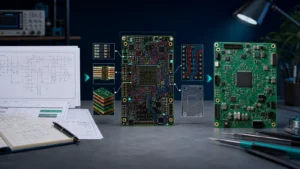
How Much Does PCB Layout Cost? PCB layout is normally quoted from engineering scope and complexity rather than one public fixed price. The workload depends on schematic size,
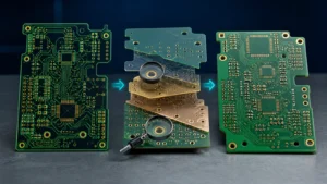
Before releasing a PCB for manufacturing, review trace and spacing constraints, drill and finished-hole requirements, annular rings, board-edge clearance, via structures, solder mask, silkscreen, the board outline, stackup,
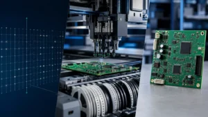
An SMT pick-and-place file should identify each placed component by reference designator, X coordinate, Y coordinate, rotation and board side. Where available, it can also include the package