
Featured Article
Embedded & FPGA PCB Design: From Architecture to Reliable Bring-Up
A practical engineering guide covering architecture, power sequencing, DDR routing, SI/PI verification, DFM, and reliable board bring-up.
Read Featured Article
A practical engineering guide covering architecture, power sequencing, DDR routing, SI/PI verification, DFM, and reliable board bring-up.
Read Featured Article
A clear, practical 22-step enterprise PCB design workflow covering project inputs, component placement, stack-up planning, routing, verification, Gerber review and production-ready file archiving.
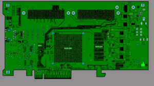
PCB layout engineering services covering placement, routing, stackup, signal and power integrity, DFM, verification, and production-ready design files.
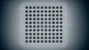
Evaluate BGA solder-joint voids by their size, location, distribution and applicable requirements. Review paste, stencil, reflow and X-ray evidence before choosing corrective actions.
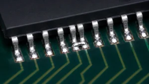
Trace unintended solder connections to printing, placement, board geometry or process conditions, then verify a controlled correction before the next assembly run.
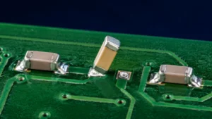
Understand why two-terminal SMT components lift during reflow and use a structured workflow to distinguish design, printing, placement and material contributors.
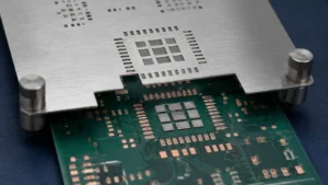
A practical stencil review covering thickness, aperture geometry, paste release and mixed-component requirements, with the inputs needed before SMT production.
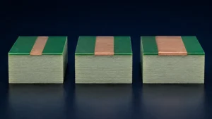
Choose PCB copper by layer with a clear view of conductor geometry, finished thickness, via transitions and manufacturing constraints. Includes a practical review checklist.
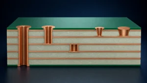
A manufacturing-focused comparison of through, blind, buried and microvia structures, with via-in-pad considerations and the inputs needed to review a multilayer interconnect.
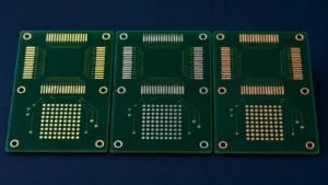
Select a PCB surface finish around soldering, pad flatness, storage, RF, contacts and wire bonding rather than assuming one finish is best for every board.
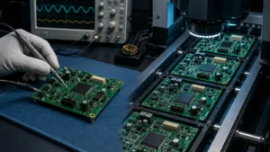
Prototype-to-production PCBA requires controlled materials, released files, repeatable tests and documented acceptance. Compare the differences and review transition readiness.
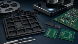
A decision guide for obsolete, EOL and hard-to-find BOM components: verify supply, assess approved alternatives, plan last-time buys and define redesign needs.

DFM, DFA and DFT address different production-readiness risks. DFM focuses primarily on whether the PCB can be fabricated reliably, DFA focuses on whether components can be assembled and
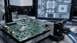
PCB assembly quality cannot usually be verified with a single method. Visual inspection and automated optical inspection (AOI) detect visible workmanship and placement defects, X-ray inspection evaluates hidden
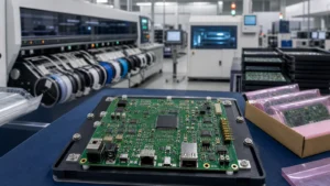
Follow the turnkey PCB assembly process from file and BOM review through sourcing, PCB fabrication coordination, SMT/THT assembly, inspection, testing, packaging, and shipment.
Understand the main PCB assembly cost drivers, what changes PCBA pricing, and which files and requirements suppliers need for an accurate quotation.

A complete PCB manufacturing file checklist covering Gerber or ODB++, NC drill data, fabrication drawings, BOM, pick-and-place files and test requirements.

How Much Does PCB Layout Cost? PCB layout is normally quoted from engineering scope and complexity rather than one public fixed price. The workload depends on schematic size,
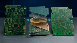
Before releasing a PCB for manufacturing, review trace and spacing constraints, drill and finished-hole requirements, annular rings, board-edge clearance, via structures, solder mask, silkscreen, the board outline, stackup,

An SMT pick-and-place file should identify each placed component by reference designator, X coordinate, Y coordinate, rotation and board side. Where available, it can also include the package

A production-ready PCB assembly BOM should identify each component by reference designator, quantity per board, manufacturer, manufacturer part number, value or description, and package or footprint. It should
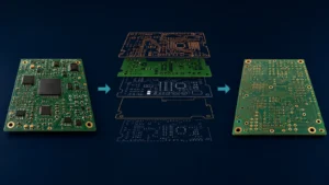
To export Gerber files from Altium Designer for PCB manufacturing, open the approved PCB document and use File » Fabrication Outputs » Gerber Files. Configure Gerber or Gerber
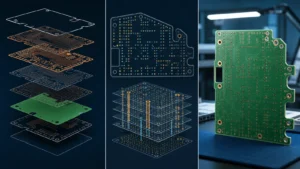
Before sending a PCB design for manufacturing, verify that the fabrication package contains the correct copper, solder mask, silkscreen, board outline and NC drill data. Confirm that the
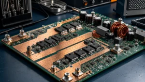
Engineering guidelines for high-current PCB layout covering copper paths, via arrays, switching loops, heat spreading, safety spacing and manufacturing.
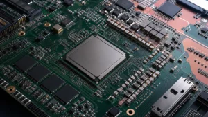
Engineering guidelines for FPGA power integrity, PDN design, decoupling placement, BGA power delivery, plane transitions, sequencing and PI validation.
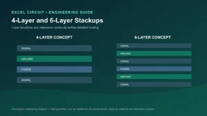
An engineering guide to PCB stackup design covering layer functions, reference planes, power distribution, materials, controlled impedance, via architecture, construction balance and manufacturing DFM.
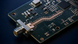
Engineering guide to 50-ohm RF PCB traces covering microstrip, stripline, coplanar waveguide, stack-up variables, connector transitions and fabrication tolerance.

An engineering guide to BGA fanout covering escape-channel planning, dog-bone routing, via-in-pad, microvias, stack-up coordination, return paths, power delivery and manufacturing DFM.
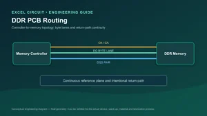
Engineering-focused DDR PCB routing guidelines covering topology, timing budgets, byte-lane constraints, length matching, impedance, return paths, SI/PI and manufacturing review.
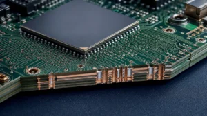
Engineering guide to via-in-pad PCB design covering fine-pitch BGA escape, microvias, VIPPO filling and capping, soldering risk, cost and DFM.

A practical engineering guide to RF PCB layout, controlled impedance, low-loss materials, grounding, transitions, simulation, testing, and manufacturable high-frequency designs.
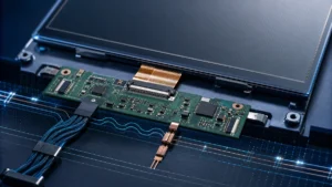
LCD and touchscreen PCB design guidance for interfaces, power, backlight, signal integrity, ESD, grounding, noise control, and layout verification.
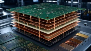
This article will take you from a beginner’s perspective to quickly understand the commonly used basic concepts in PCB design

Why PCB Layout Matters
A PCB serves as the foundation for electronic components, connecting various elements and enabling their seamless operation. The PCB layout plays a pivotal
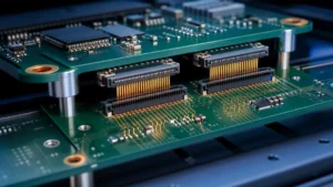
Select a board-to-board connector by pitch, current, voltage, signal integrity, stack height, mating cycles, environment, assembly, and lifecycle.
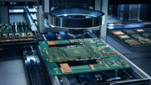
Advanced PCB manufacturing guide covering multilayer stackups, rigid-flex construction, HDI microvias, materials, DFM data, qualification, and inspection.

1. Patch device spacing This article sorts out some details that need to be paid attention to in Layout, let’s see whether you know them all !The spacing
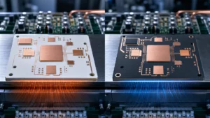
Ceramic PCB guide comparing alumina and aluminum nitride substrates, thermal performance, applications, manufacturing limits, and cost drivers.

Medical electronics SMT assembly guide covering traceability, cleanliness, process validation, inspection, testing, and supplier controls.

Prevent PCB short circuits through schematic review, layout controls, fabrication checks, SMT process control, inspection, and electrical testing.
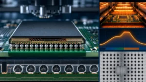
BGA assembly guide covering package structure, solder paste, placement, reflow, X-ray inspection, common defects, and process controls.

Standardize PCB design templates through controlled libraries, stackups, rules, documentation, reviews, versioning, and release governance.

Reflow soldering is an SMT assembly process in which solder paste is printed onto PCB pads, components are placed into the paste, and the assembly passes through a
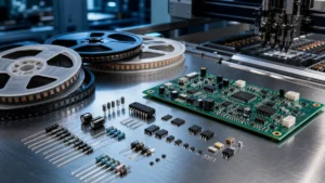
Clear definitions of BOM, DIP, SMT, SMD, THT, PCB, and PCBA, including how each term fits into PCB assembly and manufacturing files.
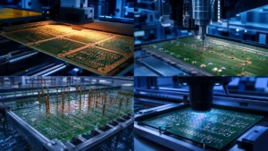
The PCB manufacturing process converts validated design data into a finished bare circuit board through imaging, etching, lamination where required, drilling, copper deposition and plating, solder-mask application, surface
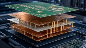
Understand PCB substrates, copper layers, prepreg, vias, solder mask, silkscreen, surface finishes, and how each structure supports circuit operation.
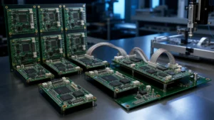
PCB design reuse standardizes verified schematic and layout modules through Altium snippets, device sheets, library control and multichannel design.