
Featured Article
Embedded & FPGA PCB Design: From Architecture to Reliable Bring-Up
A practical engineering guide covering architecture, power sequencing, DDR routing, SI/PI verification, DFM, and reliable board bring-up.
Read Featured Article
A practical engineering guide covering architecture, power sequencing, DDR routing, SI/PI verification, DFM, and reliable board bring-up.
Read Featured Article
An engineering guide to BGA fanout covering escape-channel planning, dog-bone routing, via-in-pad, microvias, stack-up coordination, return paths, power delivery and manufacturing DFM.
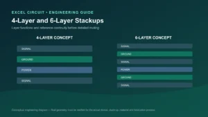
An engineering guide to PCB stackup design covering layer functions, reference planes, power distribution, materials, controlled impedance, via architecture, construction balance and manufacturing DFM.

A clear, practical 22-step enterprise PCB design workflow covering project inputs, component placement, stack-up planning, routing, verification, Gerber review and production-ready file archiving.
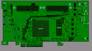
PCB layout engineering services covering placement, routing, stackup, signal and power integrity, DFM, verification, and production-ready design files.

1. Patch device spacing This article sorts out some details that need to be paid attention to in Layout, let’s see whether you know them all !The spacing
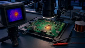
Prevent PCB short circuits through schematic review, layout controls, fabrication checks, SMT process control, inspection, and electrical testing.

Standardize PCB design templates through controlled libraries, stackups, rules, documentation, reviews, versioning, and release governance.
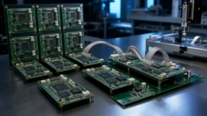
PCB design reuse standardizes verified schematic and layout modules through Altium snippets, device sheets, library control and multichannel design.