Contents
Introduction
Within HDI PCB design, via-in-pad is valuable when a component pitch, escape density, electrical path, or thermal requirement cannot be handled efficiently with conventional vias beside the pad. It is not automatically the best choice for every BGA or thermal pad. Moving a via into a land changes fabrication, plating, planarity, solder behavior, inspection, reliability, and cost.
The engineering decision must be made with the package land pattern, fanout plan, PCB stack-up, microvia structure, assembly process, and qualified manufacturer in view. Via diameter, BGA pitch, fill material, cap thickness, and stacking rules are process-dependent and should never be copied as universal dimensions.
Engineering Summary
- Use via-in-pad when it provides measurable routing, electrical, grounding, or thermal value.
- Distinguish an open via in a pad from a filled, planarized, and plated-over VIPPO structure.
- Coordinate the via type with BGA pitch, pad geometry, layer count, stack-up, and escape requirements.
- Specify fill, cap, planarity, inspection, and acceptance requirements in manufacturing data.
- Review solder-volume, voiding, reliability, sequential-lamination, and cost effects before release.
Key Design Factors
Fine-pitch BGA escape
As package pitch and ball count tighten, dog-bone fanout may not leave usable routing channels. Laser microvias placed in selected BGA pads can move signals to build-up layers with less surface congestion. However, package pin assignment, routing direction, power/ground distribution, and required layer transitions should be optimized before deciding that every pad needs via-in-pad.
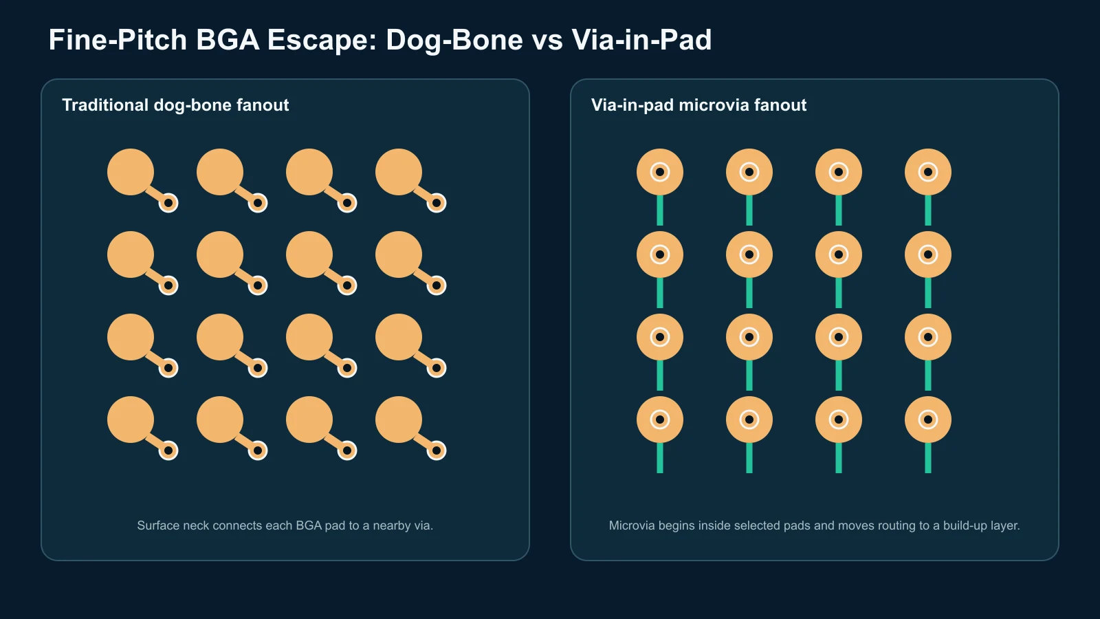
An HDI fine-pitch BGA case study provides a practical reference for coordinating escape density, microvias, stack-up, and DFM.
Via type and stack-up
A mechanically drilled through via, blind via, laser microvia, stacked microvia, and staggered microvia have different pad, aspect-ratio, registration, stub, lamination, and reliability implications. The chosen via must match the dielectric thickness and the fabricator’s qualified process. Stacked structures should not be assumed acceptable without explicit manufacturer approval.
Assembly interface
The component sees the finished land, not the drill file. Depressions, exposed fill, cap variation, voids, or incomplete plugging can affect solder paste, joint formation, coplanarity, and inspection. Surface finish, solder-mask definition, stencil design, package warpage, and reflow profile must be considered with the via structure.
Detailed Engineering Guidelines
1. Confirm that via-in-pad solves a defined problem
Use it when conventional fanout cannot meet escape capacity, when a short low-inductance connection is important, when a ground or power pad needs direct access, or when a thermal path must start inside the component land. Do not select it only because the technology is available. A pin-swapping change, layer reassignment, smaller conventional via, or revised placement may solve the problem with lower cost and risk.
2. Choose between microvia and drilled-via implementations
Microvias are often used under fine-pitch BGAs because their capture pads and build-up depth can support dense fanout. Filled and capped mechanically drilled vias may be used for larger pads, thermal lands, or other structures when aspect ratio and process allow. The correct drill, pad, and capture geometry depends on layer span, board thickness, dielectric, registration, plating, and manufacturer capability.
3. Define VIPPO correctly
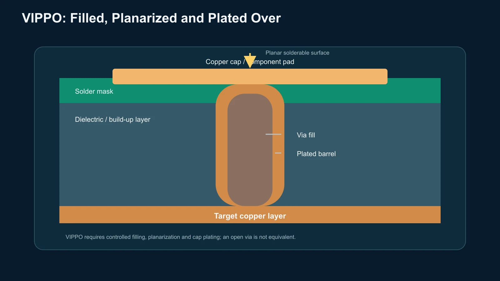
VIPPO generally refers to via-in-pad plated over: the via is filled, planarized, and covered with copper so the component land presents a solderable surface. Do not use “via-in-pad” and “VIPPO” as if they guarantee the same process. State the fill type, planarization, cap plating, finished pad requirements, surface finish, and inspection criteria on the drawing or controlled fabrication notes.
4. Select fill material around function and process
Non-conductive epoxy fill is widely used because the plated barrel carries current while the fill supports planarization and cap plating. Conductive fill may be selected for particular thermal or electrical goals, but its benefit depends on material properties, geometry, interfaces, and reliability requirements. Do not assume conductive fill automatically provides a superior thermal path; model or test the complete structure when thermal performance is critical.
5. Engineer the cap and finished land
The cap must provide a continuous, planar solderable land without creating unacceptable height variation or reliability risk. Cap requirements depend on pad size, via size, fill process, copper build, surface finish, and assembly. Agree on planarity and acceptance with the PCB and assembly suppliers. The finished component pad geometry must remain consistent with the package land-pattern strategy.
6. Use via-in-pad selectively in BGA fanout
Map signal, ground, power, clock, and sensitive analog balls before placing vias. Some package regions may escape with dog-bones while central rows require microvias. Selective use can reduce lamination cycles and cost. Preserve reference-plane continuity and avoid antipad patterns that fragment power or ground beneath the BGA.
7. Control stacked and staggered microvias
Staggered microvias distribute interfaces laterally; stacked microvias preserve a direct vertical path but place greater demands on fill, registration, plating, and process reliability. Limit stack depth according to the fabricator’s qualified technology and the product reliability requirement. Avoid approving deep stacks solely because a generic capability table lists them.
8. Separate signal, power, ground, and thermal objectives
A high-speed signal via is evaluated for stub, return path, pad capacitance, and transition impedance. A power or ground via is evaluated for current distribution and loop inductance. A thermal via is evaluated for heat flow, copper connection, fill, solder behavior, and destination copper. These functions can share a technology but should not share one unexamined rule.
9. Address soldering risks
An open or incompletely filled via can wick solder away from the land, creating insufficient solder, voiding, or joint variation. Tenting alone may not be a reliable solution for a component pad. Confirm the fabrication process, stencil aperture, paste volume, land definition, and inspection plan. For exposed thermal pads, the relationship among via openings, fill, paste segmentation, and void targets must be established with assembly engineering.
10. Document and verify the structure
Include a via table that identifies layer span, drill method, nominal geometry, fill, cap, and applicable locations. Align the drill files, pad stacks, stack-up, and fabrication notes. Define cross-section, X-ray, electrical test, microsection, or other acceptance evidence according to product risk. Ensure substitutions or process changes require approval when they affect reliability or assembly.
Common Mistakes
- Using open vias in solderable pads without an approved fill and cap process.
- Calling out “VIPPO” without defining fill, planarization, plating, and acceptance.
- Applying via-in-pad to every BGA ball before analyzing escape capacity.
- Using generic microvia dimensions that do not match dielectric thickness or supplier rules.
- Stacking more microvias than the qualified reliability process supports.
- Ignoring power-plane fragmentation caused by dense antipads.
- Treating thermal vias and RF/signal vias as the same design problem.
- Leaving assembly, stencil, voiding, and X-ray requirements until after PCB release.
Manufacturing Considerations
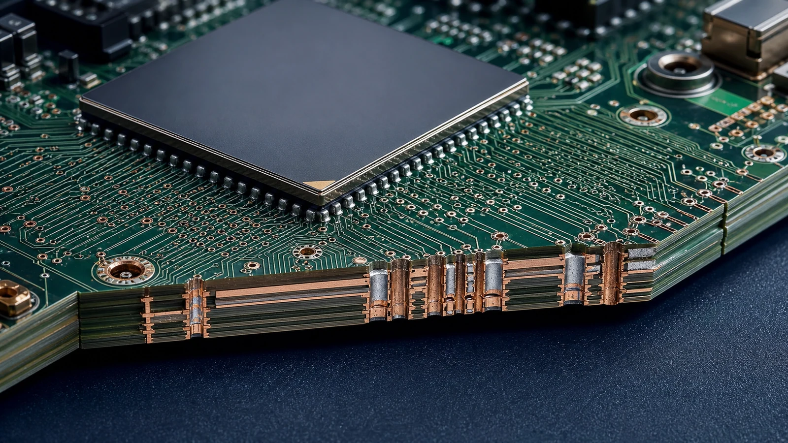
Via-in-pad can add laser drilling, sequential lamination, fill, cure, planarization, cap plating, inspection, and yield controls. The cost increase depends on board area, via count, number of build-up cycles, via type, panel utilization, material, and supplier process. Selective use may be more economical than applying the process across the entire board.
Confirm minimum laser drill, capture pad, registration, dielectric thickness, aspect ratio, fill void criteria, cap plating, and surface planarity with the selected PCB manufacturer. For high-reliability products, review microvia interface fatigue, stacked-via limitations, thermal cycling, and acceptance testing. The fabrication drawing, stack-up, and CAD pad stacks must describe the same construction.
Engineering Checklist
- Via-in-pad is tied to a documented escape, electrical, grounding, or thermal need.
- Package pitch and land pattern are checked against the actual assembly process.
- Via type, layer span, and build-up structure are manufacturer-approved.
- Fill material, planarization, cap plating, and surface finish are specified.
- Selective versus universal via-in-pad use has been evaluated.
- Stacked/staggered microvia construction follows qualified reliability limits.
- Signal transitions have an intentional return path.
- Power and ground vias do not create current bottlenecks or plane fragmentation.
- Thermal-via function and solder-paste strategy are coordinated.
- Solder wicking, voiding, planarity, inspection, and rework have been reviewed.
- Fabrication notes, via table, drill data, stack-up, and pad stacks agree.
FAQ
Does every fine-pitch BGA require via-in-pad?
No. The need depends on BGA pitch, ball map, routing channels, layer count, via capability, and pin assignment. Some packages can use dog-bone fanout throughout; others need selective or extensive microvia-in-pad escape.
Is VIPPO the same as an open via placed in a pad?
No. VIPPO is a controlled filled, planarized, and plated-over construction intended to restore a solderable pad surface. An open via can wick solder and is not an equivalent assembly interface.
Should conductive fill be used for thermal via-in-pad?
Not automatically. Thermal performance depends on the plated barrel, fill conductivity, geometry, copper planes, interfaces, and heat destination. Select the fill with the manufacturer and thermal analysis rather than relying on the label alone.
How much does via-in-pad increase PCB cost?
There is no fixed percentage. Cost depends on via technology, count, sequential-lamination cycles, fill and cap process, inspection, board complexity, yield, volume, and supplier capability. Obtain a project-specific fabrication review.
Need Help with an HDI or Fine-Pitch BGA Design?
Coordinate BGA fanout, microvia construction, filling, capping, assembly and DFM before committing to via-in-pad.