Contents
What Makes FPGA PCB Design Difficult?
FPGA PCB design is difficult because dense BGA escape, memory timing, high-speed interfaces, clocks, multiple power rails, stackup, return paths, SI/PI, and manufacturability must all work as one constrained system. A decision that helps one area can consume routing layers, via access, plane continuity, placement space, or power-delivery margin needed elsewhere. The task is not simply routing around a large package; it is resolving interacting electrical, physical, thermal, and production constraints before they become late layout changes.
The best process starts with system definition and continues through controlled production release. This guide explains what must be decided, why the decisions interact, and when to use the deeper specialist resources. Actual package, interface, pin-bank, timing, power, and manufacturing requirements must come from the selected devices, component vendors, and qualified PCB manufacturing resources.
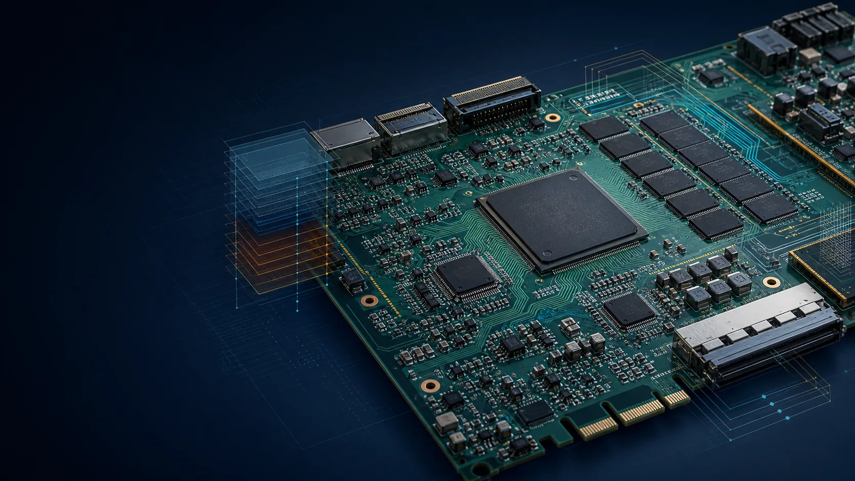
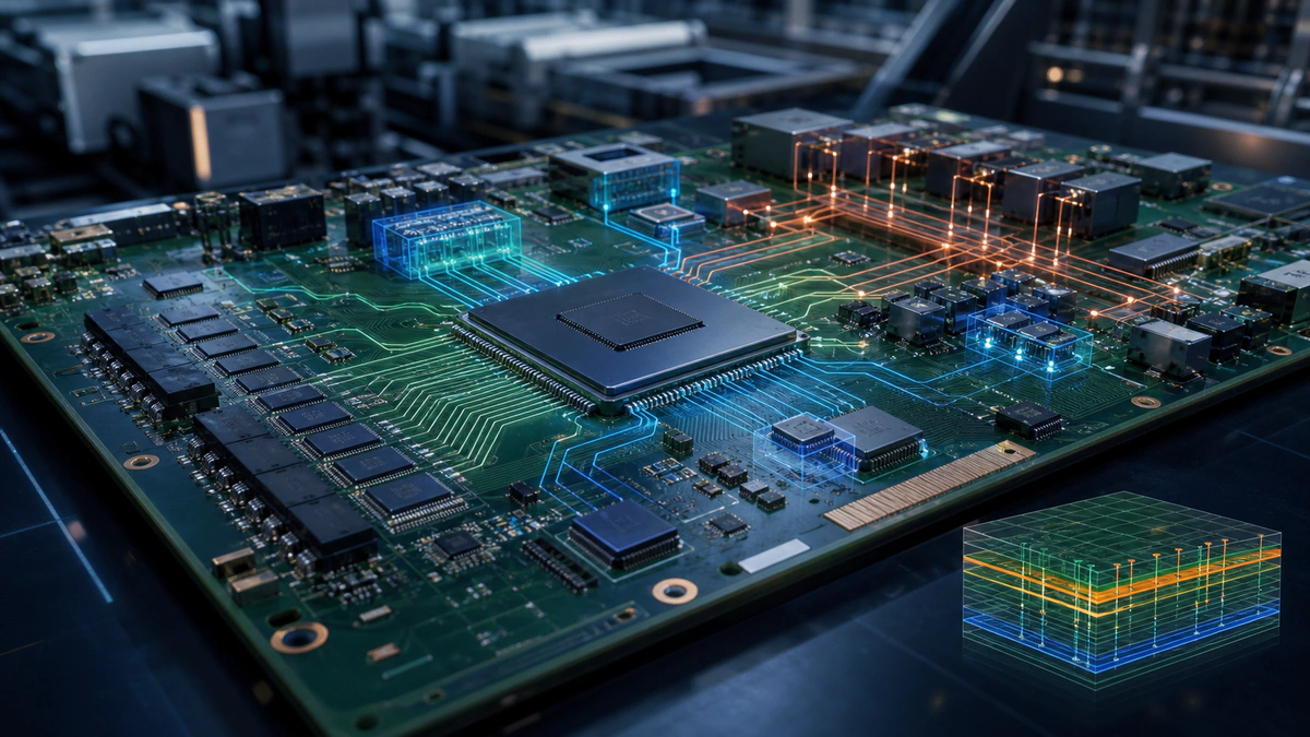
A successful embedded and FPGA PCB coordinates device architecture, memory, power, high-speed routing, stackup, and manufacturing constraints.
Define the System Before Layout Begins
What should be defined before FPGA PCB layout starts?
Before FPGA PCB layout starts, define the FPGA part and package, schematic maturity, pin assignments, I/O-bank usage, memory and high-speed interfaces, clock architecture, power rails, board outline, connector locations, mechanical limits, preliminary stackup, fabrication capability, assembly needs, and validation access. Missing inputs can force package, pinout, placement, layer, or routing changes after the physical design has already constrained the available options.
A functional block diagram should connect the FPGA or processor to memory, clocks, power, boot and configuration devices, PHYs, debug, and external connectors. For each interface, record its voltage domain, direction, topology, vendor constraints, and verification owner. Include enclosure, airflow, board-edge, mounting, connector, and production-volume constraints early enough to influence placement.
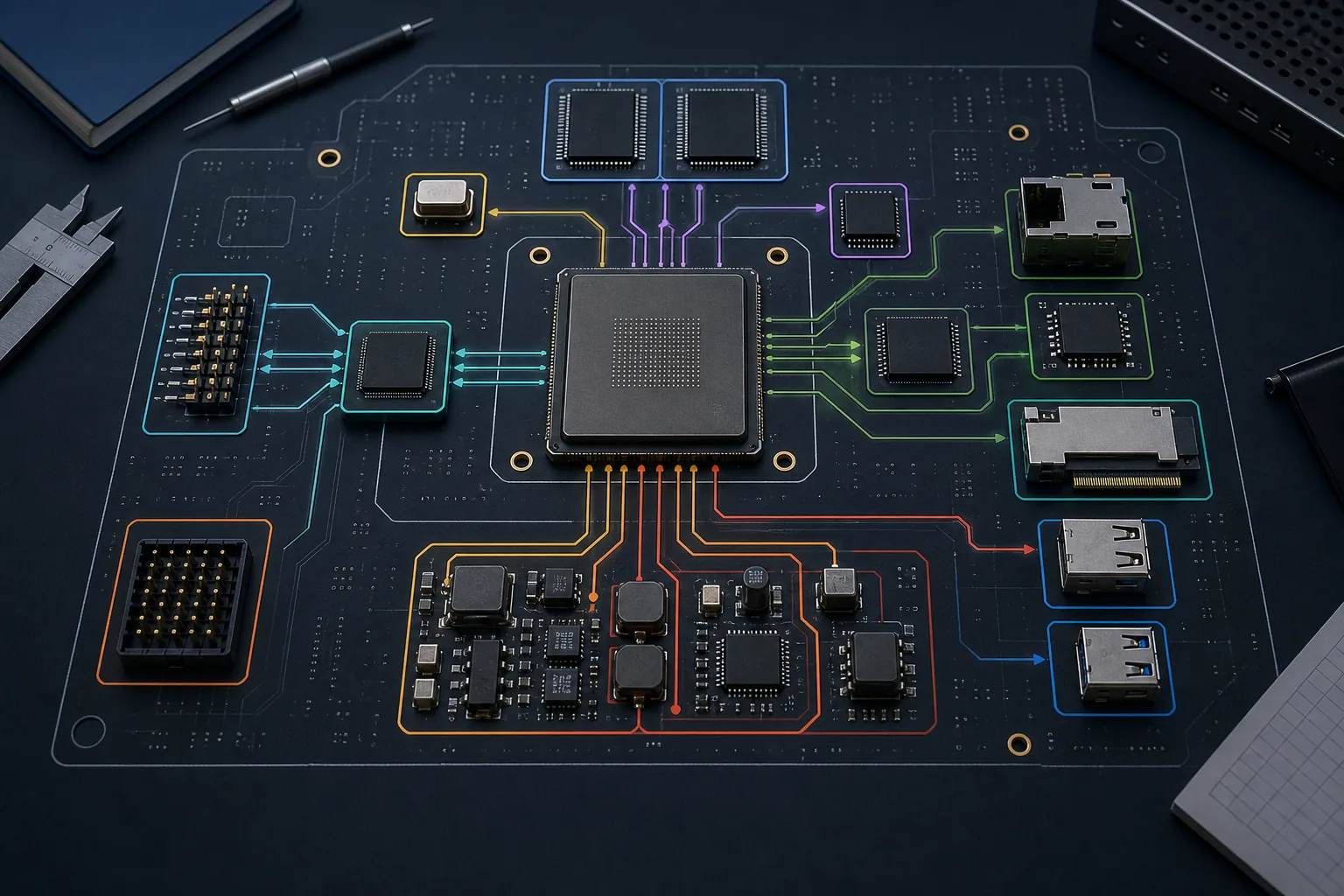
Architecture planning exposes electrical and physical dependencies before they become layout constraints.
Plan FPGA Pins, Banks, and Placement Together
Why should FPGA pin assignments be planned before layout?
FPGA pin assignments should be planned before layout because I/O-bank voltages, interface grouping, clock-capable pins, transceiver resources, memory placement, and BGA escape are physically connected decisions. A late bank or pin move can alter voltage domains, clock access, breakout direction, layer demand, and component placement. Verify every rule against the selected FPGA vendor’s package and device documentation rather than transferring assumptions from another family.
Placement determines routing feasibility. Position the FPGA, DDR or other memory, oscillators, PHYs, connectors, regulators, configuration flash, and analog support circuitry by interface priority and physical dependency. Review escape direction, return paths, power access, thermal spreading, debug reach, and mechanical obstructions before optimizing local component density. There is no universal placement distance that fits every package, stackup, or interface.
BGA Fanout and Stackup Are One Feasibility Problem
Why does FPGA BGA fanout affect the PCB stackup?
FPGA BGA fanout affects the PCB stackup because package pitch, ball count, escape density, via technology, routing channels, and reference-plane access determine how many usable signal and plane layers the board needs. The stackup in turn controls via length, trace geometry, return paths, and power distribution. Prove escape feasibility with realistic manufacturing rules before locking either the layer structure or the package.
The hub-level decision is whether the chosen package can be escaped while preserving reference and power structures. Microvias or via-in-pad may be appropriate for some dense packages, but neither is mandatory for every FPGA. Use the BGA Fanout and Escape Routing Guidelines for detailed via and breakout trade-offs, and the PCB Stackup Guide for layer planning, impedance, materials, and DFM.
System-Level Engineering Map
| Engineering area | Main design question | Detailed resource |
|---|---|---|
| BGA fanout | Can the package be escaped with feasible via and layer rules? | BGA Fanout Guide |
| Stackup | Do routing, reference, power, and manufacturing layers work together? | PCB Stackup Guide |
| DDR memory | Are placement, topology, timing, and grouping constraints satisfied? | DDR Routing Guidelines |
| Power integrity | Are rails, regulators, decoupling, planes, and BGA access coordinated? | FPGA Power Integrity |
| High-speed layout | Are topology, channel, references, transitions, and coupling controlled? | High-Speed PCB Design |
Plan DDR Memory from Controller Requirements
How should DDR memory be planned on an FPGA board?
DDR memory should be planned from the selected controller and memory constraints, beginning with placement, topology, DQ/DQS grouping, command/address relationships, reference planes, and BGA escape. Trace rules should implement the electrical timing budget rather than force every net to identical length. Include package delay when supported, keep byte-lane relationships clear, and validate the implemented geometry against the applicable device guidance.
Memory placement and breakout must be reviewed before unrelated routing consumes the direct channels. Different signal groups can have different topology and matching needs, so a single generic tolerance is not a substitute for interface constraints. The DDR Routing Guidelines covers topology, timing, length matching, references, and verification in specialist depth.
Plan High-Speed Serial Channels End to End
How should FPGA high-speed interfaces be planned?
FPGA high-speed interfaces should be planned as complete channels with defined topology, controlled impedance, continuous references, intentional via transitions, connector placement, crosstalk control, and a device-appropriate loss budget. For supported interfaces such as PCIe, Ethernet, USB, LVDS, MIPI, or SerDes, include package escape, coupling components, connectors, and any cable or backplane. “As short as possible” is not a complete routing requirement.
Pair symmetry and clean references matter, but unnecessary tuning can add loss and coupling. Model or analyze a channel when the decision risk justifies it, using models appropriate to the package, vias, connector, and transmission path. The broader High-Speed PCB Design page explains the professional engineering context, while PCB Layout Optimization provides system-level guidance on SI, EMI, thermal behavior, and return continuity.
Return Paths and Clock Architecture
Why do return-current paths matter in FPGA layouts?
Return-current paths matter because fast FPGA interface edges drive current through nearby reference structures as well as through the visible signal trace. Plane gaps, voids, poorly planned reference changes, and distant stitching paths increase loop discontinuity and can worsen coupling, common-mode current, or emissions. When a signal changes layer or reference, plan an adjacent return connection appropriate to the involved reference structures.
Clock architecture deserves its own review. Place oscillators and clock support circuitry with clean references and suitable power, keep noisy switching structures away where practical, and route clocks according to the device and clock-source requirements. Differential clocks are not required in every case; where they are used, preserve their channel and reference relationships. Do not invent frequency or jitter limits outside the selected component documentation.
Coordinate FPGA Power Integrity with Layout
Why is FPGA power integrity important?
FPGA power integrity is important because multiple rails and changing current demand must be supported through regulators, bulk and local decoupling, planes or pours, vias, package connections, and return paths. BGA breakout and stackup determine how that network reaches the device, while rail noise sensitivity and sequencing differ by FPGA family. Power delivery is therefore an architecture and placement problem, not a capacitor-count exercise.
At hub level, define each rail, its source, load assumptions, sequence, access, and sensitivity before detailed layout. Coordinate regulators, thermal paths, decoupling regions, plane continuity, and BGA power/ground escape. Use the FPGA Power Integrity guide for target-impedance concepts, installed capacitor behavior, via geometry, regulator noise, analysis, and validation.
Understand the SI, PI, and Thermal Relationship
Signal integrity and power integrity share placement, layers, planes, vias, and package structures. Reference quality affects signal return, while power and ground impedance can influence the local I/O environment. That does not make every functional failure an SI/PI problem; separate timing, signal, power, firmware, and component evidence during verification.
Thermal planning should cover FPGA dissipation, regulator heat, copper spreading, thermal vias where appropriate, airflow, heat-sink or enclosure constraints, and temperature effects on components and power conversion. Do not infer a thermal solution from package power alone. Mechanical and thermal constraints must be visible during placement, not added after routing is complete.
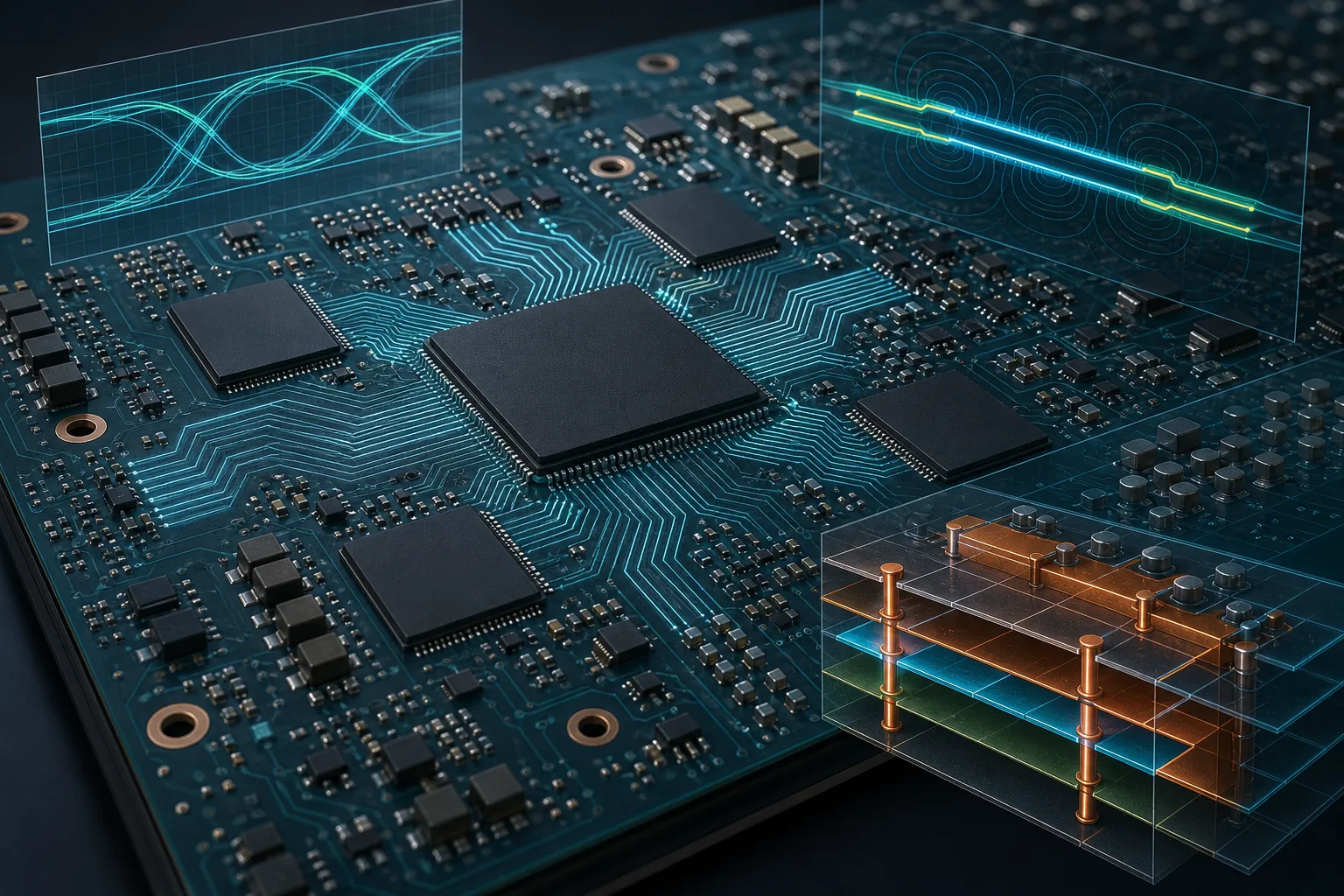
SI/PI analysis is most useful when it guides a concrete stackup, routing, via, placement, or decoupling decision.
Configuration, Bring-Up, and Recovery
Plan configuration flash, JTAG, programming headers, boot straps, reset, safe-mode access, and debug connectors as hardware requirements. Confirm that programming and recovery paths remain accessible after assembly and enclosure integration. A corrupted image or incorrect configuration should have a documented recovery route that does not depend on inaccessible BGA pins.
Bring-up access may include primary rails, power-good outputs, reset, critical clocks, boot-mode pins, configuration signals, UART, and JTAG. Define a controlled initial-power sequence, expected observations, current-monitoring approach, and functional stress cases. Measurement access and probing methods must be suited to the signal or rail being examined.
Build DFM and DFA into the Architecture
What DFM issues matter on dense FPGA boards?
Dense FPGA-board DFM must address package pitch, escape density, trace and space capability, stackup, drill and microvia construction, via-in-pad processing where used, solder-mask registration, assembly clearance, BGA inspection, X-ray access, rework, and panel constraints. Review these limits before package and layer decisions are fixed. Excel Circuit coordinates fabrication through qualified PCB manufacturing resources and performs in-house SMT assembly; it does not require one universal board technology.
Assembly review should also cover orientation, thermal-pad construction, paste apertures, fiducials, tall-part and connector clearance, component availability, and substitutions. Confirm actual fabricator rules rather than generic CAD defaults. No FPGA board automatically requires HDI, a minimum layer count, via-in-pad, or a fixed via geometry; the appropriate construction follows the package, routing, electrical, reliability, and production constraints.
Verification and Controlled Release
What should be checked before releasing an FPGA PCB?
Before releasing an FPGA PCB, verify the schematic and nets, pin assignments and bank voltages, placement, stackup, BGA breakout, DDR constraints, high-speed channels, clocks, return paths, power rails and decoupling, DRC, SI/PI analysis where justified, thermal risks, DFM/DFA, fabrication coordination, and validation access. Then independently inspect the exported manufacturing package against the approved design revision.
Production data should include the controlled source, fabrication and drill data, stackup and impedance notes, fabrication and assembly drawings, BOM and approved substitutions, centroid data, programming requirements, and applicable engineering records. Simulation is useful when it changes a design decision; it is not a universal release requirement for every FPGA board.
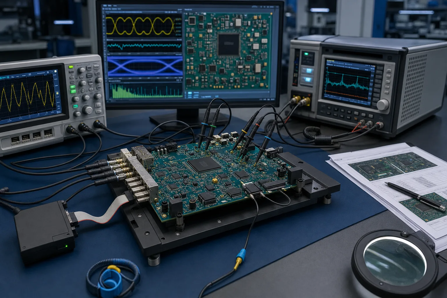
Accessible measurement points and a controlled validation plan make first-board bring-up faster and more informative.
A Practical FPGA PCB Design Flow
- Requirements: define the FPGA, interfaces, environment, mechanics, production goals, and acceptance evidence.
- Pin and interface planning: map banks, clocks, transceivers, memory, configuration, and debug.
- Placement and feasibility: arrange functional components and prove package escape with realistic rules.
- Stackup and constraints: coordinate routing layers, references, power, impedance, and manufacturing.
- Implementation: execute BGA breakout, memory, high-speed channels, clocks, power, and general routing.
- Engineering review: check return paths, SI/PI where needed, thermal behavior, DRC, and system interactions.
- DFM/DFA and release: coordinate fabrication and assembly, inspect outputs, and archive the approved package.
Common FPGA PCB Design Mistakes
- Starting layout before pin and interface planning: late pin changes can disrupt banks, placement, and breakout.
- Placing FPGA and memory independently: routing channels and timing relationships may become impractical.
- Separating BGA fanout from stackup: escape feasibility, references, and via construction are interdependent.
- Applying one DDR length rule: signal groups and device constraints can require different relationships.
- Ignoring return paths: a geometrically correct trace can still cross a reference discontinuity.
- Treating decoupling as a part count: installed impedance and current-loop geometry matter.
- Routing transceivers only for minimum length: the complete channel, loss, transitions, and coupling govern margin.
- Requiring simulation by default or skipping it by default: analysis scope should follow decision risk.
- Leaving DFM until export: package, layer, and via choices may already be expensive to change.
- Copying a reference design directly: package, pinout, utilization, interfaces, mechanics, and manufacturing constraints must be revalidated.
FPGA PCB Design Review Checklist
- FPGA part, package, migration plan, and vendor documentation confirmed.
- Pin assignments, I/O-bank voltages, clocks, transceivers, configuration, and debug reviewed.
- Memory placement, topology, grouping, and device constraints applied.
- Preliminary stackup and BGA breakout verified with realistic manufacturing rules.
- High-speed channels, references, transitions, connectors, and loss assumptions reviewed.
- Power rails, regulator architecture, sequencing, decoupling, and BGA power/ground access reviewed.
- Return paths, SI/PI analysis where needed, and thermal constraints checked.
- DFM/DFA, assembly inspection, rework access, and qualified fabricator requirements confirmed.
- Manufacturing outputs, programming data, revision control, and validation plan independently checked.
From Technical Guidance to Engineering Support
Excel Circuit’s in-house PCB design engineers support FPGA projects involving architecture, BGA breakout, stackup, DDR, high-speed routing, SI/PI, and DFM/DFA through the Embedded & FPGA PCB Design service. For a practical application of these connected decisions, review the representative FPGA & Embedded Board engineering scenario; it is an engineering example, not a claimed customer project.
Request an FPGA or Embedded PCB Review
If you are planning an FPGA or embedded PCB, share the schematic, FPGA package, pin assignments, memory and high-speed interfaces, preliminary stackup, and manufacturing constraints for engineering review.