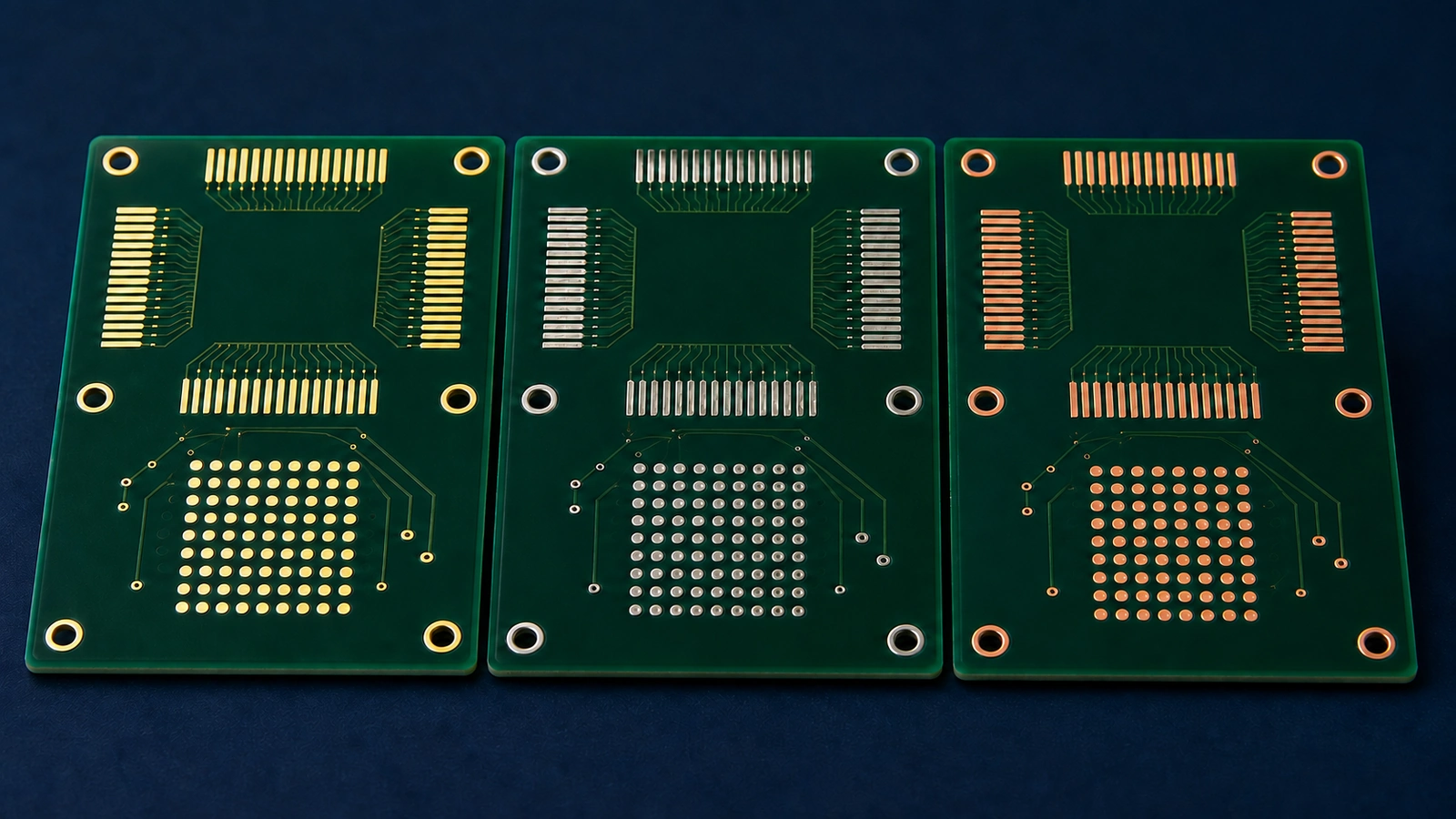
A PCB surface finish protects exposed copper and defines the surface presented to solder, contacts or a bonding process. It can affect pad flatness, fine-pitch assembly, storage and handling, and specialized RF or wire-bond applications. Choose the finish around the product’s actual assembly and use conditions; no finish is universally best.
Start with the most restrictive requirement: component pitch, soldering sequence, wire bonding, exposed contacts, RF performance or storage before assembly. Then compare the qualified manufacturing options. Selecting only by the finish name or the lowest board quote can leave an incompatible interface for the assembly team.
| Finish | Flatness | Fine-pitch / BGA | Advantages | Limitations | Selection situation |
|---|---|---|---|---|---|
| HASL, tin-lead | Less uniform than thin planar finishes | Needs geometry and process review | Established solder-coated surface | Planarity; lead restrictions | Compatible conventional assembly where tin-lead is permitted |
| Lead-free HASL | Depends on leveling capability | Review small pads and tight pitch | Lead-free solder coating | Planarity and thermal-process considerations | Compatible lead-free assemblies without demanding pad coplanarity |
| ENIG | Planar deposited finish | Common candidate | Flat pads; protected solderable surface | Nickel/gold process control; application-specific RF review | Fine-pitch SMT and defined storage requirements |
| OSP | Follows copper pad geometry | Candidate with qualified assembly | Thin copper protection; relatively simple process | Handling, thermal exposure and contact requirements | Controlled soldering and material flow |
| ENEPIG | Planar deposited finish | Candidate; not required by pitch alone | Soldering and qualified wire-bond options | More process complexity and cost | Mixed interconnect or wire-bond requirements |
| Immersion silver | Thin, planar deposit | Candidate with qualified assembly | Solderability; nickel-free finish stack | Tarnish, packaging and environmental exposure | Flat solder pads or application-specific RF requirements |
What the Surface Finish Does—and What It Does Not Do
The finish protects exposed copper between fabrication and assembly and provides a defined joining or contact interface. It is different from solder mask, which covers areas that should not normally receive solder. Copper geometry, mask openings and surface finish work together, but changing the finish does not repair an incorrect land pattern.
For soldered pads, the finish must be compatible with paste, flux and the intended soldering sequence. During joining, some finish layers dissolve or participate in the metallurgical interface. An unsoldered contact or wire-bond pad has a different function and may need a specifically qualified finish rather than the board’s default solderable surface.
Flatness is also a system property. A planar deposit cannot compensate for board warpage, package coplanarity problems or inconsistent paste printing. State the assembly requirement first, then ask whether the selected finish and manufacturing process support it.
HASL and Lead-Free HASL: Review the Pad Geometry
Hot air solder leveling (HASL) coats exposed copper with solder and removes excess material using hot air. Conventional HASL commonly refers to a tin-lead process; lead-free HASL uses a lead-free solder alloy. Specify which is intended rather than placing an ambiguous “HASL” note on a lead-free build.
The resulting solder surface is familiar to many assembly processes, but its thickness and local shape depend on the leveling process and pad geometry. Fine-pitch devices and small lands can be less tolerant of uneven deposits. Review the assembler’s requirements rather than declaring every HASL board unsuitable for every BGA.
Lead-free HASL also requires an appropriate thermal process. Confirm compatibility with the board construction and the later assembly sequence. It can be a practical choice for suitable conventional assemblies, but a modest fabrication saving is not useful if pad planarity creates placement or printing difficulty.
ENIG: Flat Pads With a Controlled Nickel/Gold Interface
Electroless nickel immersion gold (ENIG) places a nickel barrier over copper and a thin gold layer over the nickel. Its planar surface makes it a common candidate for fine-pitch SMT and BGA pads. The protective finish can also support storage before assembly when packaging and handling remain controlled.
ENIG quality depends on the actual deposition process. Excessive nickel corrosion, often discussed as “black pad,” is a process-control concern that can compromise solder-joint integrity; it is not an inevitable feature of every ENIG board. Neither a gold-colored appearance nor a generic finish label demonstrates compliance with a specified deposit requirement.
Ask the qualified fabricator to confirm the applicable finish specification and verification approach. Do not substitute an assumed thickness value from an online comparison chart. Nickel-based finishes also deserve application-specific review when an exposed conductor forms a significant part of a high-frequency path.
OSP: A Solderable Copper Surface Needs Controlled Handling
Organic solderability preservative (OSP) uses a thin organic coating to protect copper from oxidation before soldering. It does not add the nickel/gold metal stack of ENIG. The coating follows the underlying copper geometry and can support fine-pitch soldering when the assembly process is qualified.
Handling and the complete thermal sequence matter. Multiple reflows, selective soldering, rework, storage between operations and the chosen flux can change the demands on remaining unsoldered pads. Confirm the coating supplier’s and assembler’s process window rather than assuming either that OSP tolerates every sequence or that it is limited to a single reflow.
The iNEMI surface-finishing overview discusses how OSP chemistry and assembly exposure affect performance. For a production decision, request the qualified handling and thermal limits for the process actually being supplied. A general coating family is not a storage guarantee.
OSP should not be treated as a durable wear surface for repeated mechanical contacts. If test probes or contacts must touch protected copper before soldering, identify that use explicitly and verify the intended contact method.
ENEPIG: Consider It When the Interconnect Requires It
Electroless nickel electroless palladium immersion gold (ENEPIG) adds palladium between the nickel and gold layers. It provides a planar surface and can support soldering and qualified wire-bond processes. The extra deposition stage increases process complexity; its value depends on the interfaces the product actually needs.
Wire-bond compatibility is not established by the acronym alone. Wire material, bonding method, finish condition and the qualified process must work together. MacDermid Alpha’s ENEPIG technical information describes wire-bond applications for its finish system. That capability still requires qualification for a particular substrate and assembly.
A fine-pitch board using only conventional solder joints does not automatically require ENEPIG. Ask what requirement it satisfies that another qualified finish cannot. Avoid upgrading a finish solely because the product is described as “advanced” or “high reliability.”
Immersion Silver: Flatness With an Exposure Plan
Immersion silver deposits a thin silver layer on exposed copper. Its planar surface and solderability make it a candidate for fine-pitch assembly. The finish stack does not add a nickel barrier, which can be relevant when assessing exposed RF conductors.
Silver surfaces require appropriate packaging, handling and environmental control. Tarnish and contamination can affect the condition presented to assembly or contacts. Confirm approved packaging, storage conditions and the action required after a package is opened or its condition is uncertain. Do not assign a universal shelf life to every immersion-silver board.
MacDermid Alpha’s immersion-silver information identifies soldering and electrical-contact applications for qualified systems. For a customer drawing, specify the required function and acceptance conditions, not just “silver” as an appearance requirement.
Surface Finish for BGA, QFN and Fine-Pitch Assembly
Small pads make the relationship between finish uniformity, paste printing and placement more important. BGA and QFN selection should consider the package’s land pattern, pitch, pad definition and assembly process together. Planar finishes are often candidates, but the finish cannot correct an unsuitable stencil or an unqualified reflow profile.
The BGA assembly and inspection guide covers the surrounding soldering and verification issues. Here, the finish decision should establish what surface the paste and component will encounter and whether that condition remains acceptable through the planned operations.
Ask the assembler to review the actual smallest or most sensitive features, not only the nominal package family. A board containing both fine-pitch joints and large thermal pads can present different printing and soldering constraints within the same assembly.
Surface Finish in RF and Contact Applications
A surface finish can change the electrical behavior of an exposed conductor, but its significance depends on frequency, geometry, finish stack and the length of conductor affected. Nickel conductivity and the distribution of high-frequency current are reasons to evaluate the finish; they are not grounds to reject ENIG for every RF product.
Determine which parts of the RF path are actually exposed and finished. Review transmission lines, launches, pads and contacts with the complete stackup and loss budget. A finish change may need simulation or measurement on representative hardware. The RF PCB design guide provides the wider context for materials, geometry and verification.
Contacts require a separate functional check. Repeated mating, sliding wear, low-level signals and wire bonding may need different surface properties. A solderable immersion-gold surface should not automatically be specified for a connector wear surface. State the contact mechanism so the fabricator can review a suitable qualified finish, including selective treatment where appropriate.
How to Select the Right Finish
Use the product’s limiting requirement to narrow the options, then verify the complete manufacturing sequence before release.
- Identify the interface. Separate solder pads, test contacts, mating contacts and wire-bond areas.
- Review sensitive geometry. Identify the smallest pitch, BGA/QFN features and any coplanarity concerns.
- Define thermal exposure. Include both sides of assembly, selective soldering and planned rework where relevant.
- Define storage and handling. State the expected delay to assembly, packaging requirements and exposure after opening.
- Check application-specific behavior. Include RF loss, contact performance, wire bonding and the product environment.
- Compare qualified manufacturing options. Assess process capability, inspection requirements, availability and cost within the actual quote.
- Record the approved finish. Align the drawing, fabrication notes and assembly requirements; require review before substitutions.
For example, a solder-only fine-pitch control board may narrow its options around flatness and the assembly sequence. A board with wire-bonded devices starts with bond-process compatibility. An exposed RF structure adds a loss evaluation. These are different decision paths even if the boards use the same laminate.
The PCB DFM guidelines connect the selected finish with the rest of the fabrication requirements. Keep the finish choice in the controlled release rather than allowing it to change silently during quotation.
Common Selection Mistakes
- Choosing only by board price. Consider assembly compatibility, verification and the consequence of an unusable surface.
- Assuming one shelf life for a finish family. Use the supplier’s qualified packaging and storage conditions.
- Treating finish changes as cosmetic. Review soldering, contacts, bonding and RF consequences before approval.
- Ignoring the second assembly operation. An acceptable initial surface must also support the remaining unsoldered features.
- Using unspecified “gold” for every interface. Solder pads, wire bonds and wear contacts can require different structures.
Information Required From the Customer
Provide the information that determines the joining or contact requirement:
- Requested finish, or the finishes permitted by the drawing.
- Relevant fabrication data and drawing notes identifying exposed pads and special areas.
- Smallest component pitch, BGA/QFN requirements and known assembly constraints.
- Soldering sequence, alloy or process restrictions and expected thermal exposures.
- RF requirements and the relevant stackup when the finish affects an exposed signal path.
- Contact or wire-bond function, including the process that must be qualified.
- Storage, packaging and product-environment requirements.
- Applicable specification and revision, target quantity and any customer approval restrictions.
If the finish is undecided, describe the required function instead of selecting an acronym to complete the order form. That allows the review to compare appropriate options without assuming requirements that the product does not have.
Review the Finish Before PCB Fabrication
Excel Circuit coordinates PCB manufacturing through qualified resources, with engineering review of the fabrication and assembly requirements. A useful finish review identifies the controlling application, confirms a qualified process and records the agreed specification before production.
Send the relevant Gerber data, fabrication notes and assembly requirements for a surface-finish review. Include the stackup when RF behavior or construction makes it relevant, and identify any contact or wire-bond areas. Request a fabrication and surface-finish review.