Contents
Before releasing a PCB for manufacturing, review trace and spacing constraints, drill and finished-hole requirements, annular rings, board-edge clearance, via structures, solder mask, silkscreen, the board outline, stackup, controlled impedance where applicable, and special fabrication requirements. Acceptable limits depend on the board construction, copper weight, material, layer structure, fabrication process, and selected manufacturer’s capability. A manufacturability review should therefore compare the actual design and release intent with the process intended to build it.
What Is PCB Design for Manufacturability?
PCB design for manufacturability, commonly called PCB DFM, is the review of a PCB source design and its manufacturing intent before fabrication release. The purpose is to determine whether the materials, geometry, drilling, plating, solder mask, routing, stackup, and special processes can be interpreted and produced using the intended fabrication process. It connects design decisions with practical production capability while there is still time to resolve ambiguity or revise the layout.
DFM is related to design rule checking, but the two are not identical. A DRC checks whether the board violates rules already defined in the PCB CAD environment. Those rules may cover clearances, widths, hole sizes, layer use, or connectivity. A clean DRC result is important because it shows that the design satisfies its configured rule set, but it does not independently prove that every rule reflects the selected material system, copper construction, drill process, or fabricator capability.
A DFM review goes further by asking whether the configured rules and resulting geometry are appropriate for the real manufacturing route. Both DRC and automated DFM can be software-assisted. DFM may also require manufacturing engineering judgment when the answer depends on registration, plating, lamination, routing, mask processing, yield margin, or a special feature that software cannot interpret from geometry alone.
The review should be based on the intended board rather than a generic rule list. A standard rigid board, an HDI build, a heavy-copper design, and a controlled-impedance RF board can require different checks. When the design contains unusual geometry or an uncertain process choice, a PCB DFM review can help align source data, fabrication notes, and manufacturing assumptions before release without turning the technical checklist into a substitute for project-specific engineering.
Quick PCB DFM Checklist
Use this checklist as a release review framework. It identifies areas that normally require confirmation, but it does not prescribe universal dimensions. Record project requirements and confirm uncertain limits with the selected fabricator.
| Area | What to Check | Why It Matters |
|---|---|---|
| Trace width / spacing | Geometry by layer, copper weight, density, and local neck-down | Etching capability and process margin vary with the construction |
| Copper-to-edge clearance | Copper near routed edges, cutouts, slots, and V-score lines | Edge processing can affect nearby conductors and exposed copper |
| Annular ring | Pad, intended finished hole, and registration relationship | Drilling and plating must leave a usable plated feature |
| Drill and finished-hole requirements | Finished dimensions, tolerances, and plating intent | The production drill tool may differ from the finished opening |
| PTH / NPTH identification | Clearly distinguish plated and non-plated holes and slots | Ambiguous plating intent can change mechanical or electrical function |
| Via structure and layer pairs | Via type, start/stop layers, fill, cap, and plating where applicable | Advanced vias may change lamination and processing |
| Solder mask openings / webs | Pad openings, narrow webs, exposed copper, and fine-pitch areas | Mask registration and process capability affect the finished result |
| Silkscreen and polarity marks | Text, references, pin-one marks, polarity, and pad interference | Legend should remain readable without contaminating exposed pads |
| Board outline, slots and cutouts | Closed profile, internal geometry, dimensions, and plated intent | The fabricator must identify the finished board shape unambiguously |
| Copper distribution | Large imbalances, isolated copper, planes, and layer-to-layer distribution | Distribution can influence processing and dimensional behavior |
| Stackup and material requirements | Layer order, thickness, copper, material, and dielectric intent | The physical build must support electrical and mechanical requirements |
| Controlled impedance | Target nets, layers, references, targets, and final stackup | Impedance depends on coordinated geometry and material properties |
| Surface finish | Project finish, selective areas, contacts, and assembly needs | The correct finish depends on use, assembly, and material requirements |
| Fabrication notes | Notes agree with PCB data, drawings, and the current revision | Conflicting instructions create avoidable interpretation risk |
| Special processes | Edge plating, castellations, controlled-depth routing, press-fit, or other features | Special features may require dedicated documentation and process approval |
| Manufacturer capability alignment | Confirm critical features against the intended production process | A capability limit is not automatically a recommended design rule |
| Revision consistency | Source data, outputs, drawings, notes, and stackup share one revision | Mixed releases can invalidate an otherwise correct review |
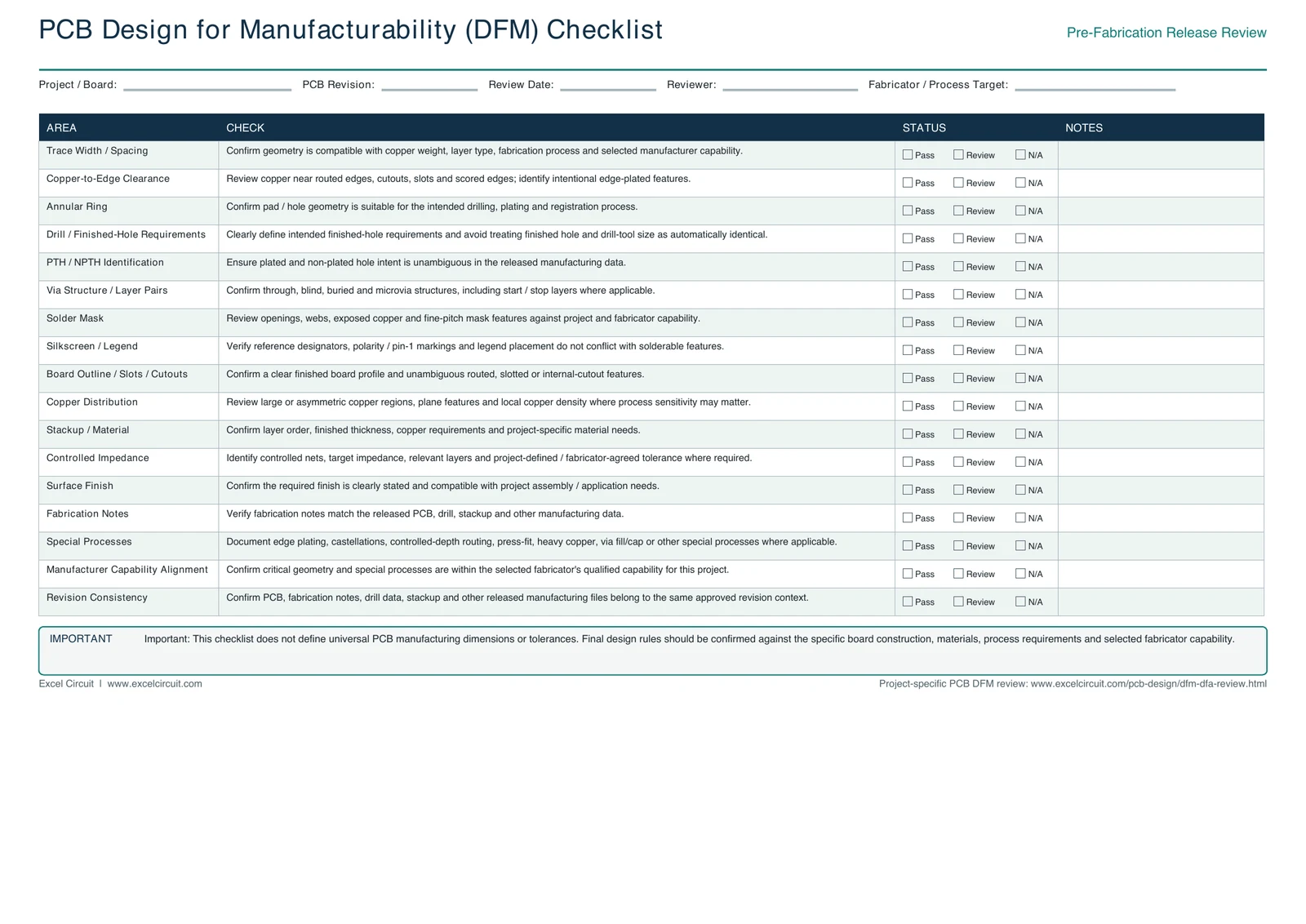
Download the PCB DFM Checklist
Use this one-page printable checklist to review key PCB manufacturability items before fabrication release. Final dimensions and tolerances should still be confirmed against the project requirements and selected fabricator capability.
1. Check Trace Width and Spacing
Trace width and spacing should be reviewed in the context of routing density, copper weight, layer type, and the selected etching process. Inner and outer layers do not necessarily behave identically during fabrication, and heavier copper can change the practical geometry that a process can reproduce with useful margin. A rule that is acceptable for one construction may therefore be inappropriate for another even when the CAD system reports no violation.
Pay particular attention to fine-pitch component areas, dense escapes, neck-down regions, and transitions between general routing and locally constrained geometry. Local neck-down may be justified when it is limited to the area required to leave a pad field, but it should be intentional and included in the review. Check that pours, teardrops, clearances, and rule priorities do not create unexpected narrow features in the manufacturing output.
Design rules should not be selected only because a fabricator lists a feature as technically possible. Designing exactly at a fabrication capability limit can reduce process margin and may increase manufacturing sensitivity. The more of the board that relies on a limiting feature, the more important it becomes to confirm how copper construction, layer selection, quantity, and production expectations affect acceptance.
If a project requires very fine geometry, coordinate it with the intended fabricator before routing is frozen. Ask whether the stated value is a capability limit, a routinely supported production rule, or a project-specific result that depends on additional controls. Preserve agreed values in the PCB rules and release documentation so later revisions do not silently return to unrelated defaults.
2. Review Copper-to-Board-Edge Clearance
Review copper near every finished routed edge, not only the rectangular outline visible in the main board view. Internal cutouts, routed slots, notches, tabs, and mechanical openings can create additional finished edges. Where V-scoring is used, inspect copper relative to the score path and intended separation process. Copper pours and planes deserve the same attention as individual traces because they can approach an edge without being visually obvious at normal zoom.
The required separation depends on the routing process, copper type, plating requirement, mechanical design, and fabricator capability. Exposed copper close to an edge may be affected differently from covered internal copper, while a mechanically critical area may need its own project constraint. Instead of applying one universal clearance, define an appropriate project rule and verify exceptions against the expected finished profile.
Some designs intentionally place copper at or around the board edge. Edge plating, edge contacts, and castellated features are intentional exceptions rather than ordinary clearance violations. Identify these features explicitly in the fabrication documentation, show their location and plating intent, and confirm the production method with the fabricator. An exception that is clear in the designer’s mind but absent from released data can be interpreted as an error or removed during routine correction.
3. Check Annular Ring and Hole Geometry
For a plated through hole, review the relationship between the pad diameter, intended finished hole, annular ring, and surrounding clearances. The finished feature depends on drilling, registration, plating, and board construction. A pad that appears centered and adequate in the source design still needs to remain functional after normal manufacturing variation is considered.
Finished hole size is not necessarily the same as drill tool diameter. A plated hole receives copper during processing, so the fabricator may select a production drill based on the requested finished opening, plating build, drill behavior, and its qualified process. Designers should specify the intended finished hole and any functional tolerance that matters to the component lead, press-fit requirement, fastener, or mechanical interface. Manufacturing drill selection can then be made by the fabricator using its process controls.
Do not treat drill compensation or annular ring as one fixed value for every technology. Review small holes, dense connectors, press-fit arrays, slots, heavy-copper layers, and holes close to board edges or copper features as project-specific cases. Registration requirements may also differ across layer counts and constructions. Where available pad geometry is constrained, discuss the feature before release rather than assuming a nominal CAD relationship will be accepted unchanged.
Check that libraries and drawings use the same finished-hole intent. A footprint copied from another project may carry a hole or pad definition created for a different lead, tolerance, or process. Confirm the mechanical requirement first, then align the footprint, PCB data, drill information, and fabrication notes so the manufacturer is not forced to infer which value controls.
4. Separate PTH and NPTH Requirements Clearly
A plated through hole (PTH) has conductive plating on the hole wall and normally provides an electrical or structural connection through the board. A non-plated through hole (NPTH) is produced without that conductive wall and is commonly used for mechanical alignment, mounting, tooling, or hardware where plating is not intended. The labels describe manufacturing intent; they should not be assigned solely from the visual appearance of a circular opening.
PTH and NPTH features must be clearly distinguishable in the released fabrication data. This does not mean they must always be supplied in two separate drill files. Separate outputs are one possible workflow, but attributes, fabrication drawings, notes, tool definitions, or another manufacturer-accepted method may communicate the distinction. The correct method is the one that makes plating intent unambiguous to the receiving process.
Review mounting holes, connector retention features, plated and non-plated slots, locating holes, and other mechanical openings. Confirm whether pads, copper keepouts, grounding, or plating are intended around each feature. Slots require particular care because their geometry and plating status may be represented differently by different CAD exports. Resolve unclear classifications before release rather than relying on the manufacturer to infer them from context.
5. Review Via Structures
Via selection affects drilling, plating, lamination, routing density, cost, and inspection. Review each via type against the stackup and confirm that fabrication data communicates its actual layer connectivity. Do not assume that a via name in the design library is enough; the released structure and layer-pair intent must be understandable to the fabricator.
Through, Blind and Buried Vias
A through via extends through the finished board and can connect copper layers along that path. A blind via begins on an outer layer and terminates on an internal layer. A buried via connects internal layers without reaching either finished outer surface. These structures can require different drilling and lamination sequences, so the start layer, stop layer, and intended connection must be defined correctly.
A blind via is not automatically a microvia. “Blind” describes which surfaces or layers the via reaches, while “microvia” is associated with a particular class of small, typically laser-formed interconnect used in an HDI process. A design can therefore contain a blind structure that should not be described or manufactured as a microvia. Use terminology that reflects the intended construction and confirm it against the fabricator’s process.
For special via structures, document the applicable layer pair, plating requirement, and sequential lamination implications where they apply. Check that the stackup supports access to the intended layers during fabrication. If multiple blind or buried structures are used, review whether their combinations introduce additional build cycles or inspection requirements. These decisions are best coordinated before routing is frozen because a late change to the via architecture can affect escape routing and layer allocation.
Microvias and Via-in-Pad
Microvias are commonly associated with HDI manufacturing and may be used to support fine-pitch escape routing, short layer transitions, or compact interconnect structures. Stacked and staggered arrangements can have different process and reliability implications, and their use should be coordinated with the selected build-up sequence. A project that depends on these structures should align layer architecture, material system, and fabrication route early in the design.
Via-in-pad places a via within a component or land-pattern pad. It can improve routing access or electrical performance in appropriate designs, but the required treatment depends on assembly and design intent. Not every via-in-pad must always be filled and capped. If filling, capping, or planarization is required to prevent solder loss, support assembly, provide a flat pad, or satisfy another project need, that requirement should be explicitly documented.
When via-in-pad, stacked microvias, staggered microvias, or sequential lamination are part of the architecture, review them with the fabricator and assembly process rather than selecting a generic library default. For a deeper design-service context covering these structures, see HDI PCB design. The goal at this stage is to make the construction explicit, not to turn the release checklist into a complete HDI tutorial.
6. Check Solder Mask Design
Review solder mask as manufacturing data, not only as a colored layer in the PCB editor. Confirm intended pad openings, areas of exposed copper, via tenting or opening, and any mask-defined or non-solder-mask-defined features required by the component or board design. Inspect the generated mask output to ensure that clearances, rule priorities, and merged openings produce the intended result.
Fine-pitch component areas and narrow mask webs deserve particular attention. Whether a web can be produced reliably depends on mask registration, the selected mask process, component pitch, pad geometry, and fabricator capability. A universal expansion or minimum sliver should not be applied without regard to those conditions. Where separate openings merge, decide whether that result is acceptable for the assembly design and confirm uncertain features with the manufacturer.
Check exposed copper beyond component pads, including test points, edge contacts, thermal features, grounding areas, and intentional mask openings. Also review vias under or near components to confirm whether they should be tented, exposed, filled, or treated in another project-defined way. The solder mask file should agree with copper, drill, and assembly intent rather than being treated as an isolated cosmetic layer.
Finally, review the actual manufacturing output at useful zoom levels. Look for unintended openings, slivers, clipped features, mask over pads, and differences between the source view and exported data. If a feature approaches the selected fabricator’s process boundary, resolve it before release and record the agreed treatment in the design rules or fabrication documentation.
7. Review Silkscreen and Legend
Review the silkscreen and legend for identification, orientation, and readability after fabrication. Reference designators should remain associated with the correct components, while pin-one indicators, polarity marks, and connector-orientation symbols should be clear enough to support assembly and inspection. Check both top and bottom legend data so that side-specific information cannot be mistaken when the board is viewed or handled during production.
Look for text, lines, or symbols that overlap solderable pads, test points, edge contacts, or other exposed copper. A PCB editor may show the intended text even when the fabrication process clips or removes parts of the legend near a mask opening. Inspect the exported legend together with solder mask and copper data, and confirm that critical identifiers remain understandable after any manufacturer-specific clearance processing.
Silkscreen capability depends on the selected fabrication process, legend method, and manufacturer capability. Do not assume one font height, line width, or clearance works for every board. Dense layouts may require moving, abbreviating, or omitting noncritical text, but orientation and safety-critical markings should be coordinated with the complete documentation rather than reduced until their meaning is lost.
Silkscreen does not replace the assembly drawing, BOM, or formal polarity requirements. For ICs, diodes, LEDs, electrolytic capacitors, connectors, and other orientation-sensitive parts, pin-one and polarity information should agree across the PCB data, legend, assembly drawing, and approved component documentation. The objective is consistent manufacturing communication, not merely an uncluttered graphic layer.
8. Verify Board Outline, Slots and Cutouts
The fabrication package should identify one unambiguous finished board profile. Review the outline as a closed contour and check corners, arcs, notches, internal cutouts, routed slots, and other mechanical features for gaps, duplicate segments, or overlapping geometry. A visually small discontinuity can be difficult to notice in the CAD view but may prevent automated tooling from interpreting the intended route.
Confirm the size, position, and plating intent of internal cutouts and slots. Plated slots and non-plated slots serve different electrical or mechanical purposes and must remain distinguishable in the released data. Connector features, mounting interfaces, tabs, and unusual routing should also agree with the mechanical drawing or product enclosure information where those references control the finished shape.
Do not prescribe one mechanical-layer number for every project. CAD systems, library standards, and company templates use different layer conventions. If multiple mechanical layers contain outline-like geometry, fabrication notes or drawings should state which data represents the finished board profile and which layers contain dimensions, keepouts, component courtyards, or reference information.
Distinguish the individual board outline from a panel outline when panel data is part of the release. The manufacturer should be able to determine whether the supplied geometry describes one finished PCB, a customer-defined panel, or supporting panelization information. This review does not require a full panelization specification, but conflicting profiles should be resolved before fabrication rather than left for interpretation.
9. Review Copper Distribution and Plane Features
Review large copper areas, plane regions, and local copper density across the stackup. Highly concentrated copper on one area or layer can behave differently during imaging, etching, lamination, and thermal processing than a more distributed design. Large or highly asymmetric copper distributions can increase process sensitivity in some board constructions and should be reviewed with the fabricator when relevant; they do not automatically mean that the board will warp or fail.
Inspect plane connections, isolated copper, narrow connections into large regions, and thermal relief where the electrical and assembly design requires it. Verify that intended plane connectivity survives polygon settings, clearances, layer assignments, and manufacturing-output generation. Isolated copper should be evaluated for its purpose instead of retained or deleted solely by a generic rule.
There is no universal copper-balance percentage or density threshold suitable for every PCB. Material, layer count, copper weight, board dimensions, and lamination construction can all affect the review. The design team should identify conspicuous asymmetry and electrically important plane features, while the fabricator may apply qualified process adjustments such as tooling or copper-balancing features where its workflow permits.
Any proposed fabrication adjustment must preserve electrical spacing, impedance, isolation, creepage, antenna, high-voltage, and mechanical requirements. If an area must remain free of added copper, communicate that intent explicitly. Copper distribution review is therefore a coordinated engineering check, not a requirement that the designer personally add the same balancing pattern to every design.
10. Confirm the PCB Stackup
The stackup defines the physical order of conductive and dielectric layers and connects electrical assumptions with the producible board construction. Confirm it before release so the PCB design, fabrication requirements, and quotation describe the same board. Gerber layer names alone may indicate artwork order, but they do not necessarily communicate finished thickness, copper requirements, material family, dielectric construction, or every process-dependent detail.
Layer Order and Finished Thickness
Document the layer sequence and identify signal, plane, and mixed-function layers clearly. Confirm the intended finished board thickness, inner- and outer-layer copper requirements, and material family when the project depends on a particular material property. Layer naming should agree between the source design, fabrication drawing, output files, and any impedance information.
Finished thickness may include tolerances and process contributions that are specific to the chosen construction. Mechanical constraints such as card guides, connectors, enclosures, or edge interfaces should be stated when they control the acceptable result. Likewise, copper requirements should distinguish project intent rather than relying only on a default stackup name inherited from a different design.
When Detailed Stackup Definition Matters
For a conventional PCB, the fabricator may propose a manufacturable production stackup from the required layer count, finished thickness, copper requirements, material class, and qualified process. The customer does not necessarily need to define every core, prepreg, and dielectric thickness. What matters is that the proposed construction satisfies the project’s electrical, mechanical, material, and reliability requirements and is approved before production.
More detailed coordination is important for controlled impedance, high-speed digital, RF, HDI, unusual materials, or tightly constrained mechanical thickness. In these cases, routing geometry and via architecture may depend directly on the production construction. Confirm the stackup before fabrication release and, ideally, before routing decisions become difficult to change. If the agreed construction requires layout revision, PCB design and layout services can support updates while keeping the technical requirements tied to the approved production stackup.
11. Document Controlled Impedance Requirements
Controlled impedance requirements should identify the target impedance, whether the structure is single-ended or differential, the applicable nets or net classes, routing layers, reference planes, and the relationship to the final production stackup. Use the project-defined tolerance or a tolerance agreed with the fabricator rather than treating one tolerance as universal.
Gerber trace geometry alone does not necessarily tell the fabricator which traces require impedance control. The same visible width may be used for ordinary routing and controlled structures, while final impedance also depends on dielectric properties, dielectric thickness, copper thickness, reference-plane geometry, and process effects. Provide an impedance table, fabrication drawing note, controlled-net identification, or another manufacturer-accepted instruction that makes the requirement explicit.
Confirm that the layer references in the impedance requirement match the released stackup. A target assigned to one signal layer and reference plane can become invalid if the production stackup changes the layer order or dielectric separation. Differential requirements should also identify the intended pair and applicable geometry without assuming the manufacturer can reconstruct design intent from two adjacent traces.
Coordinate impedance with the fabricator before release when material options, trace adjustments, or construction changes may be necessary. The fabricator may recommend geometry compatible with its qualified process, but any change should be reviewed against routing space, coupling, return paths, and the electrical design. This section addresses manufacturing communication; it does not replace signal-integrity analysis or interface-specific routing design.
12. Confirm Surface Finish and Copper Requirements
Copper Requirements
Specify inner- and outer-layer copper requirements in a way that the fabricator can relate to the intended construction. Where the project controls finished copper, state that requirement clearly. Starting copper and finished outer copper are not necessarily the same because outer-layer processing may add copper through plating. The exact relationship depends on the fabrication route and should not be reduced to one universal conversion.
Heavy-copper designs and mixed copper requirements need early coordination because they can affect etching, spacing, hole plating, stackup, thermal behavior, and finished thickness. A nominal copper-weight label should not be treated as an exact fixed final thickness for every process. Use project requirements and fabricator-confirmed construction data when the finished copper result is electrically, thermally, or mechanically significant.
Surface Finish
Define the required surface finish in the fabrication requirements, quotation data, drawing, or controlled notes. Common options include ENIG, lead-free HASL, OSP, and project-specific finishes. No one finish is universally best: the appropriate selection depends on component pitch, assembly process, contact requirements, shelf life, environment, cost, and other project constraints.
Identify selective finishes, edge contacts, exposed copper, or areas that require different treatment. Confirm that solder mask, finish, and plating instructions do not conflict. When a finish is important to assembly or product performance, do not rely on a filename or an informal quotation assumption; include it in the approved release information.
13. Document Special Fabrication Requirements
Special fabrication features should be documented whenever their complete intent cannot be inferred from ordinary copper, drill, mask, and outline data. Depending on the project, the release may need to identify:
- Edge plating, edge contacts, or castellated holes
- Controlled-depth routing, countersinks, or counterbores
- Press-fit holes and their functional finished-hole requirements
- Heavy copper or layer-specific copper requirements
- Selective surface finishes or special plating areas
- Special laminates, rigid-flex constructions, or material restrictions
- Blind or buried vias and their layer pairs
- Sequential lamination, stacked or staggered microvias
- Via filling, capping, or planarization where required
Use fabrication drawings, controlled notes, layer-pair tables, detail views, or another manufacturer-accepted method to communicate the requirement. The correct documentation depends on the feature and receiving workflow. Do not assume every manufacturer will automatically recognize a special process from geometry alone or apply the same default treatment.
Confirm feasibility, inspection method, and any design adjustments with the intended production source. Special-process capability can vary with material, dimensions, stackup, quantity, and supplier qualification. Review the proposed construction against actual PCB manufacturing services and qualified process capability before the release is frozen, while preserving project requirements rather than adapting them silently during quotation.
Common PCB DFM Mistakes
- Designing at capability limits without process margin. A listed capability limit is not automatically a preferred production rule. Using limiting geometry throughout a design can increase process sensitivity. Confirm whether a feature is routinely supported for the intended construction and production context.
- Conflicting or ambiguous board outlines. Duplicate contours, open profiles, or several mechanical layers with outline-like geometry can make the finished shape unclear. Identify the controlling board profile and keep supporting mechanical information distinguishable.
- Confusing finished-hole size with drill-tool size. Plating and the qualified drilling process affect the relationship between the production tool and finished opening. Specify the functional finished-hole intent instead of prescribing an unsupported fixed compensation.
- PTH or NPTH intent is unclear. Mounting holes, slots, and connector features can be manufactured incorrectly when plating status is ambiguous. They do not always require separate drill files, but the accepted release method must distinguish them clearly.
- Special via requirements are incomplete. A via label alone may not communicate layer pair, fill, cap, plating, planarization, or sequential-lamination needs. Document the attributes that control the actual construction.
- Copper is too close to routed or scored edges. Traces, planes, or pours may approach a route, cutout, or V-score without an appropriate project rule. Review clearance according to the fabrication method, feature purpose, and selected manufacturer’s capability.
- Solder-mask features exceed process capability. Narrow webs, small openings, and fine-pitch geometry can be affected by mask registration and processing. Inspect the real output and coordinate sensitive areas without assuming a fixed expansion or sliver rule.
- Silkscreen interferes with pads or orientation marking. Legend over exposed copper can be clipped or contaminate assembly information. Keep reference, pin-one, polarity, and connector-orientation signals readable and consistent with assembly documentation.
- Stackup and impedance are not coordinated before release. Routing may be completed using one assumed construction while production uses another. Align controlled nets, reference planes, geometry, materials, and the approved production stackup.
- Fabrication notes and released files belong to different revisions. A current PCB database can be paired accidentally with an older drawing, drill output, stackup, or note set. Review the release as one controlled package whenever manufacturing-relevant design data changes.
A DFM review should compare the PCB design, fabrication requirements, and intended full PCB manufacturing process together rather than treating any single exported file as the complete source of manufacturing intent.
DRC vs DFM Review
DRC checks whether the PCB design complies with rules configured in the CAD environment. DFM checks whether the design and release requirements are compatible with the intended fabrication process and manufacturing capability. Passing DRC is necessary in many workflows, but it does not by itself confirm manufacturability. Automated DFM tools and engineering review can both contribute to DFM.
| Check | DRC | DFM |
|---|---|---|
| Trace / spacing | Compares geometry with configured width and clearance rules | Checks rules and geometry against the intended copper and etching process |
| Hole geometry | Checks configured pad, hole, and clearance relationships | Reviews finished-hole intent, drilling, plating, registration, and capability |
| Board-edge clearance | Checks geometry against a defined edge rule | Confirms the rule suits routing, scoring, plating, and mechanical intent |
| Solder mask | Checks configured mask expansions and clearances | Reviews openings and webs against mask registration and process capability |
| Stackup | Uses the layer structure and rules entered in the design | Confirms that the intended physical construction is producible and approved |
| Controlled impedance | Can enforce geometry when suitable rules are configured | Coordinates targets, nets, layers, materials, references, and production stackup |
| Special processes | May check explicitly modeled constraints | Checks whether special intent is documented and supported by the process |
| Manufacturing capability | Depends on the accuracy of the configured rule set | Compares the release with the selected fabricator’s qualified capability |
The two checks work best together. DFM findings may lead to revised CAD rules, and a final DRC can confirm that resulting layout changes remain internally consistent. Neither process should be treated as permission to ignore electrical, mechanical, assembly, or reliability requirements.
When Should a PCB DFM Review Be Performed?
1. During Rule Definition
Confirm fabricator constraints early when the design uses an unusual stackup, HDI structures, controlled impedance, special material, heavy copper, or fine geometry. Early alignment helps the rule set represent a plausible production process before those assumptions become embedded throughout the layout.
2. Before Final Routing Freeze
Review manufacturing-sensitive geometry before routing is treated as final. Check dense escapes, neck-downs, via architecture, board-edge regions, mask features, and stackup-dependent routing while changes can still be made without disrupting the complete release.
3. Before Fabrication Release
This is the key point for a complete DFM review. Confirm that the source design, fabrication requirements, approved stackup, mechanical intent, and manufacturing package describe the same revision and leave no unresolved process assumptions.
4. After Meaningful Design Changes
Reassess DFM after a manufacturing-relevant change affects geometry, holes, stackup, impedance, solder mask, board outline, material, or fabrication data. A minor text edit does not automatically require a complete rerun, but changes that can alter the manufactured result should be reviewed and released under consistent revision control.
What Files Are Useful for a PCB DFM Review?
A useful DFM review can often begin with the available design and fabrication data, but the exact package depends on the project stage and board complexity. Files should be current, revision-consistent, and accompanied by any requirement that cannot be understood from geometry alone. Not every item below is mandatory for every review.
PCB Source Data
When a project is still in the design stage, PCB source data can help an engineer inspect routing, via definitions, board-outline intent, layer assignments, stackup assumptions, design rules, and component or footprint context. Source data can make corrections easier, but it is not always required when the review scope is limited to released manufacturing data.
Gerber or ODB++ Data
Gerber or ODB++ data represents the fabrication artwork or manufacturing release that the receiving process will interpret. It can be reviewed for layer content, outline interpretation, mask intent, and consistency with the stated construction. Use the Gerber file checklist separately when verifying the completeness of a release package; this DFM review remains focused on whether the design and manufacturing intent are practical.
NC Drill Data
NC drill data helps reviewers confirm hole locations, drill-to-copper relationships, slots, and plated or non-plated intent where that information is available. Drill data is normally supplied separately from Gerber artwork; it should not be assumed to be included automatically simply because the copper and mask layers are present.
Stackup Information
Stackup information becomes especially important for multilayer, controlled-impedance, high-speed, RF, HDI, and special-material boards. It helps connect layer order, copper requirements, material intent, thickness, via architecture, and electrical assumptions to a buildable production construction without repeating a complete stackup-design analysis.
Fabrication Drawing and Notes
A fabrication drawing or controlled notes can communicate finished thickness, surface finish, copper requirements, special via instructions, slots, cutouts, tolerances that are genuinely project-defined, and special-process requirements. The format and level of detail can vary; the important point is that the notes agree with the current design data and do not create a competing revision.
Controlled Impedance Requirements
Where impedance control applies, provide target impedance, applicable nets or net classes, routing layers, reference planes, and any project-defined or fabricator-agreed tolerance. This information allows the reviewer to relate electrical intent to the proposed production stackup instead of attempting to infer controlled structures from trace geometry alone.
Special Process Information
Identify special processes such as edge plating, castellated holes, via filling or capping, sequential lamination, controlled-depth routing, press-fit features, or heavy copper. Include the functional intent and relevant location or layer information so the review can evaluate the requirement against an actual manufacturing route.
Need a Manufacturability Review Before Release?
If your PCB design or fabrication package still needs review, submit the available project files so manufacturability risks, unclear requirements, and release inconsistencies can be identified before production. View PCB DFM Review Services.
Frequently Asked Questions
What is DFM in PCB design?
PCB DFM is the review of a PCB design against practical fabrication requirements, materials, geometry, and manufacturer capability before production release. It checks whether the design can be interpreted consistently and whether the intended construction is compatible with the selected process. The review can cover routing, holes, vias, mask, outlines, stackup, and special features. It complements electrical and layout verification by adding manufacturing context rather than replacing those checks.
What is the difference between PCB DRC and DFM?
DRC checks a PCB design against rules configured in the PCB CAD environment, such as width, clearance, hole, and connectivity constraints. DFM checks whether the resulting design and release requirements are suitable for the intended manufacturing process and capability. Passing DRC does not automatically confirm manufacturability because the configured rules may not include every material, drilling, plating, mask, stackup, or special-process constraint. Automated tools and engineering review can contribute to both workflows.
When should I perform a PCB DFM review?
Consider DFM during rule definition and perform a coordinated review before fabrication release. Early review is particularly useful for unusual stackups, HDI, controlled impedance, special materials, or fine geometry. Reassess the relevant DFM checks after a meaningful manufacturing-related change affects holes, vias, board outline, mask, stackup, impedance, or fabrication data. A minor text edit does not necessarily require a complete review when it cannot affect the manufactured result.
Does passing DRC mean a PCB is manufacturable?
No, not necessarily. DRC confirms compliance with the rules configured in the design environment. Manufacturing feasibility also depends on the actual fabricator process, material system, stackup, drilling, plating, solder-mask process, board-edge method, and special-process capability. A useful rule set can reduce risk, but DFM is still needed to compare those rules and the released design with the production route intended for the board.
What files are needed for a PCB DFM review?
A DFM review can use the available PCB source data, Gerber or ODB++ artwork, NC drill files, stackup information, fabrication drawings or notes, and project-specific manufacturing requirements. The exact package depends on the design stage, board complexity, and review scope. Source data can help while changes are still being made, while released manufacturing data shows what the fabricator will receive. The files should represent one identifiable revision.
Can a PCB manufacturer review a design before fabrication?
Yes. Many PCB manufacturing workflows include engineering or CAM review before production, although the scope varies by supplier, board technology, and project. The review can identify unclear fabrication requirements, missing data, manufacturability concerns, or inconsistencies between files and notes. It does not guarantee that every design error will be found or that manufacturing will be risk-free, so electrical, mechanical, assembly, and project-specific verification remain necessary.
Ready to Release Your PCB for Manufacturing?
Send your available PCB files, stackup, and fabrication requirements for engineering review and quotation. If some manufacturing details are still being finalized, include the current release package and identify any special process or DFM concerns.