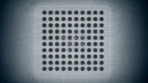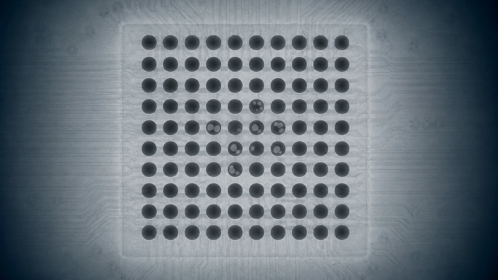
BGA voids are gas-filled or unfilled regions within solder joints that may form during reflow. Small voids can occur even in controlled processes. Their significance depends on size, location, distribution, joint function and the product’s reliability requirements. A visible void is not automatically a failed joint, and a low overall void area is not proof of acceptable long-term performance.
Evaluate the joint against the agreed customer specification and applicable standard before choosing a corrective action. The objective is a repeatable, acceptable assembly, not necessarily zero visible voids in every ball.
| Observation | Potential concern | What to review |
|---|---|---|
| Small dispersed voids | Variation within the joint population | Distribution, measurement method and application |
| Large central projected void | Reduced solder cross-section in the observed region | Actual location, joint geometry, paste and reflow |
| Clustered voids | Concentrated loss of solder continuity | Image interpretation, material condition and process consistency |
| Suspected interface-adjacent void | Possible interaction with the attachment region | Depth-resolving evidence and relevant reliability requirement |
| Repeated pattern across BGAs | A systematic design or process contributor | Ball location, stencil, surface condition and thermal history |
What Is BGA Voiding?
BGA voiding describes an absence of solder within a ball-grid-array joint. The joints sit beneath the package, so normal visual inspection cannot characterize their interiors. X-Ray imaging can reveal regions with different material attenuation, but the image still needs interpretation against the package and board geometry.
A void differs from an open joint, where the intended electrical connection is absent, and from a bridge, where solder creates an unintended connection between conductors. These conditions can coexist. An image that reveals voids should not distract the reviewer from checking alignment, joint formation and neighboring connections.
Record the affected reference designator and ball coordinates. A statement such as “this BGA has voids” is too broad to connect the finding to a particular signal, power connection, mechanical location or manufacturing pattern.
Why Voids Form During Reflow
Voids can form when gases remain trapped as solder coalesces and wets the mating surfaces. Flux volatilization, reaction products and the timing of solder flow can all contribute. Paste condition, surface solderability and the geometry available for gas escape affect that sequence.
Indium’s study of SMT voiding mechanisms links void formation with entrapped flux outgassing and solderability. It provides a mechanism to investigate, not a universal prediction for every modern paste, alloy or BGA package.
Review the material and process combination actually used. A changed paste lot, prolonged handling, different surface condition or altered thermal history may be more informative than the final void percentage alone. Some voids may also originate in the supplied solder-ball structure; comparing incoming or reference material can help distinguish package history from board-assembly effects.
Reflow atmosphere may change oxidation and wetting behavior. Treat an atmosphere change as a controlled process variable, not a guaranteed cure or an assumption about available equipment.
Stencil and Paste Deposits Influence the Starting Condition
Stencil thickness, aperture geometry and print transfer determine the additional solder paste presented to the BGA. The package balls already supply solder, so paste volume must be considered with the complete joint construction.
Excessive or inconsistent deposits can change solder flow and the amount of flux beneath the package. Insufficient transfer may introduce a different joint problem even if an X-Ray image appears to show fewer voids. Reducing paste solely to improve a void number can therefore make the assembly less acceptable.
Compare intended aperture volume with actual print evidence. Review missing deposits, position, board support and repeatability across the BGA array. Use the stencil thickness and paste-transfer review for the detailed geometry decision. Keep a record of the paste-layer and stencil revisions used for each trial.
Reflow Profile Effects Depend on the Assembly
The reflow profile controls the sequence of heating, flux activity, solder melting, wetting and solidification. A useful review examines measured temperatures at representative assembly locations rather than relying only on oven zone settings.
Preheat and any soak influence temperature equalization and material activity. The time above liquidus must support joint formation within the constraints of the alloy, paste, package and PCB. Outgassing must be considered alongside wetting: extending a stage without understanding the material can exhaust useful flux activity or expose components to unnecessary thermal stress.
Cooling influences solidification and must remain compatible with the defined process. No single preheat, soak, peak or cooling recipe is correct for every BGA assembly. Compare the measured profile with the relevant supplier guidance, then validate any change through both inspection and the required product tests.
Keep loading conditions and measurement locations consistent when comparing builds. A profile change and a simultaneous paste change make it difficult to identify which variable caused the observed result.
Check PCB Pads and Package Solderability
Pad and ball surfaces influence wetting and the opportunities for gases to escape. Oxidation, contamination, handling damage or an unsuitable surface condition can change joint formation even when printing and oven settings remain unchanged.
Review PCB finish, storage history, package condition and the actual land pattern. A finish name alone does not establish solderability; age, handling and process history also matter. The PCB surface-finish selection guide explains the wider material tradeoffs without treating a finish change as a universal voiding remedy.
Where vias enter a land, confirm the specified via treatment and the fabricated result. An opening can affect solder retention or gas behavior. Escalate an unexpected via or pad condition to the board and package reviewers rather than compensating for it with an undocumented assembly adjustment.
What X-Ray Inspection Can and Cannot Establish
Two-dimensional X-Ray provides a transmission projection through the assembly. It can show a void pattern and support area measurement, but overlapping structures can obscure details. A dark or bright feature must be interpreted using the system’s display convention and the surrounding geometry.
Oblique views can help separate overlapping features. CT or other suitable three-dimensional methods can provide additional location information when resolution and reconstruction quality support the question. They are escalation tools, not a reason to assume every routine inspection requires CT.
Keep acquisition settings, magnification, segmentation and the measurement region consistent. A projected void-area fraction is not automatically a void-volume fraction. Nor does an X-Ray image prove electrical function, thermal performance or lifetime reliability. The assembly inspection and testing comparison explains why complementary evidence is needed.
Interpret Location Without Inventing a Reliability Ranking
Void location matters because different parts of a joint can experience different mechanical, thermal and electrical conditions. The same reported area may describe one large region, several dispersed regions or a cluster close to an attachment interface.
A feature near the center of a top-down image is not necessarily centered through the joint’s depth. If interface proximity would change the disposition, obtain evidence capable of resolving that question. Do not assign a depth from the projection alone.
Compare the finding with the joint’s role and the product’s loading conditions. Avoid ranking all central voids as harmless or all edge features as failures. The useful output is a documented observation, its uncertainty and the requirement against which it must be assessed.
Establish Acceptance Criteria Before Making a Pass/Fail Decision
There is no single universal acceptable BGA void percentage for all joints and applications. Acceptance must follow the customer agreement and the applicable standard, revision, product class and joint category. A remembered number from another project is not a sufficient disposition basis.
Confirm which documents govern the assembly and how conflicts are resolved. If an IPC document is specified, use the controlled applicable edition and its actual scope. This article does not reproduce IPC acceptance tables or substitute a generic limit for the contractual requirement.
Define the measurement as well as the limit: individual void or total projected area, individual joint or a different region, image method, treatment of overlap and any location-specific requirement. Otherwise two inspectors may report different results from the same joint.
A QFN exposed thermal pad is not an ordinary BGA ball joint. Do not transfer thermal-pad coverage or voiding requirements directly to a BGA array. Similarly, a power or thermal connection may require application-specific evaluation beyond a general workmanship observation.
Separate acceptance from improvement. A process may meet the agreed acceptance requirement yet still show a trend worth investigating. Conversely, an improved average does not authorize acceptance of an individual joint that fails the governing requirement. Unclear requirements require clarification before release, not a threshold chosen after viewing the result.
Reduce Voiding Through a Controlled Prevention Plan
Void reduction should preserve the other requirements for a sound joint. Start with stable inputs and a measurable baseline, then select changes that address the observed mechanism.
- Paste: follow the supplier’s storage, preparation and working-life instructions; identify lots and handling history.
- Stencil and printing: verify aperture condition, registration and transfer consistency, including interruptions or restarts.
- Components and PCB: control handling and solderability; follow applicable package storage requirements without inventing a universal bake procedure.
- Reflow: verify the measured profile on the relevant assembly and retain the approved process definition.
- Feedback: compare X-Ray results using the same measurement method and check for new opens, bridges or other defects.
Document the changed variable, expected effect and evidence needed to accept it. Retain the trial data so the next production run can reproduce the accepted condition.
A Practical BGA Voiding Root-Cause Workflow
Use the defect pattern to narrow the investigation before changing tooling or material.
- Identify the BGA, affected ball coordinates, PCB revision and build lot.
- Review the original X-Ray images and confirm the measurement method.
- Compare locations, orientations, lots and unaffected examples.
- Inspect paste-print data for volume, position and missing deposits.
- Check stencil thickness, apertures and the actual released revision.
- Review paste storage, preparation, working time and material changes.
- Compare measured reflow profiles and loading conditions.
- Evaluate PCB and package surface condition, including relevant via features.
- Run a controlled trial that addresses the strongest supported hypothesis.
- Verify the void result and the complete joint/test requirements before approving the change.
Do not use a selected good image as evidence that the process is corrected. Compare a defined set of relevant joints and retain unfavorable results as well. Reworked units should be identified separately because their thermal history differs from the original production process.
Information Required From the Customer
A useful review package connects the images to the exact assembly configuration:
- Released Gerber or ODB++ data, paste layer and assembly revision.
- BOM, Pick and Place data, BGA part number and package information.
- X-Ray images with reference designators, ball locations and measurement details.
- Stencil data, paste identification and available print records.
- Measured reflow profile and relevant lot or handling history.
- Customer acceptance criteria and any specified IPC document, revision and class.
- Joint function, product environment and required reliability evidence where relevant.
Identify whether the request is an acceptance review, process improvement or failure investigation. Those decisions need different evidence. The DFM, DFA and DFT review framework helps assign the design, assembly and test questions to the appropriate review.
Review the Evidence Before the Next BGA Build
Excel Circuit combines in-house PCB design engineering and SMT assembly support with component sourcing and qualified PCB manufacturing resources. A focused review should establish what the images show, what requirement applies and which input needs verification.
Send the PCB data, BGA package information, X-Ray results and acceptance requirements for a BGA assembly and voiding review before the next build. Submit your BGA voiding review inputs.