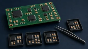
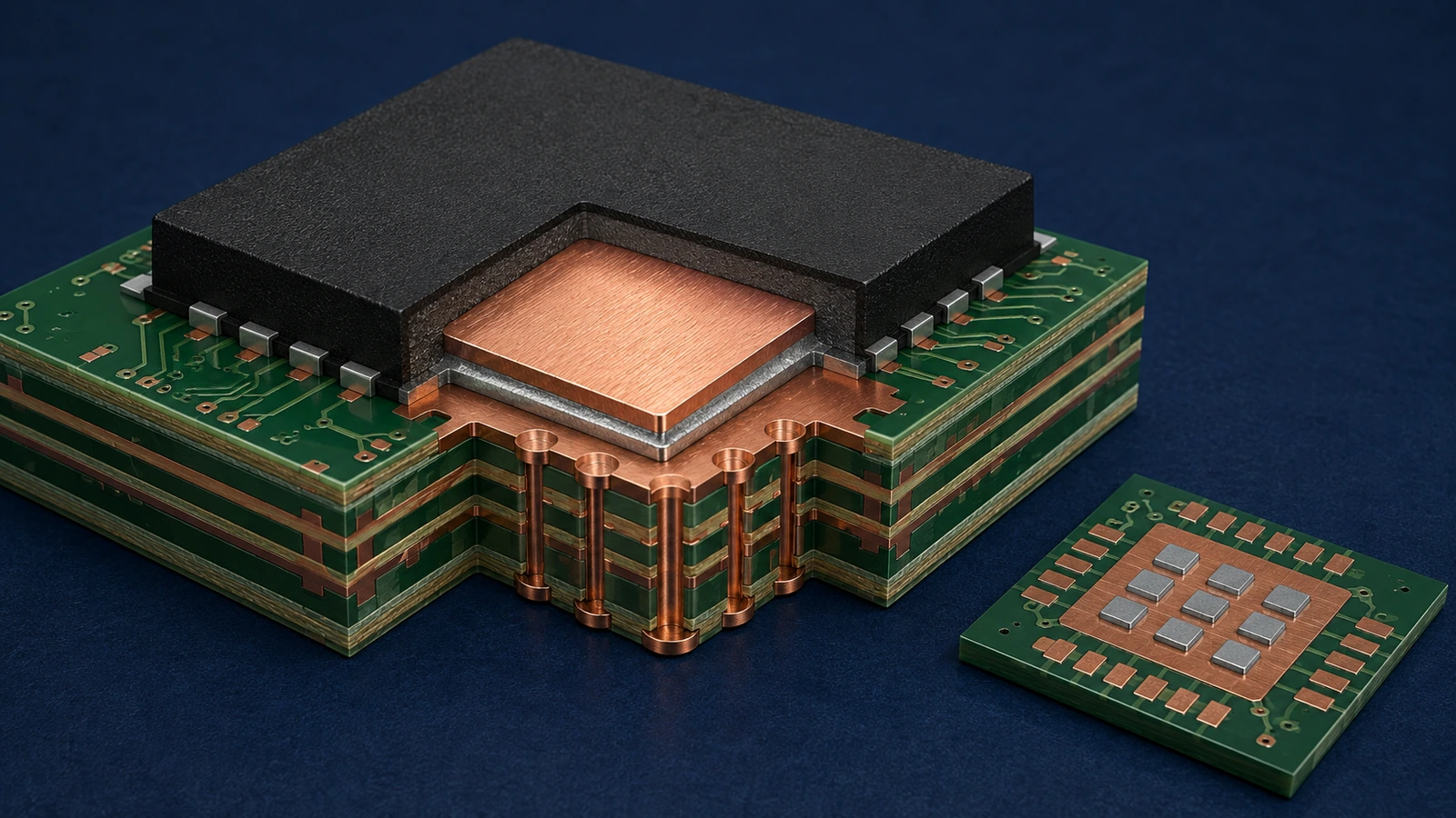
Reliable QFN assembly depends on balancing perimeter-pad joints, exposed thermal-pad solder volume, thermal vias, paste distribution, component standoff, reflow and inspection access. Too much center-pad solder can contribute to component float, excessive standoff and poor perimeter connections. Too little solder can reduce the effective thermal or mechanical attachment. Voiding also depends on material, geometry and process conditions, so changing paste coverage alone does not guarantee a sound result.
Start with the exact package datasheet and its assembly guidance. Then review the copper, solder mask, via treatment and stencil as separate but connected design decisions.
| Design element | Primary purpose | Risk to review |
|---|---|---|
| Perimeter pads | Electrical and mechanical attachment | Opens, inadequate solder or poor alignment |
| Exposed pad | Thermal path and specified electrical connection | Float, incomplete attachment or unfavorable void distribution |
| Thermal vias | Connect the surface land to internal heat-spreading structures | Solder loss into open holes or an inadequate thermal path |
| Stencil apertures | Control paste volume and distribution | Excess, insufficient or inconsistent deposits |
| Solder mask | Define intended solderable regions and separation | Unintended connections or restricted attachment area |
| Reflow process | Form the center and perimeter joints | Uneven wetting, incomplete joints or trapped gases |
What Makes QFN Assembly Difficult?
QFN packages place their electrical terminations beneath or close to the body edge instead of using long projecting leads. Many also have an exposed center pad. The resulting low standoff leaves limited space for observing the solder joints or correcting an imbalance after placement.
The center and perimeter deposits interact during reflow. A design can appear correct when each pad is considered separately yet produce an unsuitable assembled height when the deposits are combined. The review must therefore consider the package as a whole.
Related DFN or SON packages may present similar issues, but their detailed requirements are not interchangeable. Confirm the exact outline and termination design. A generic library name such as “QFN” does not identify the dimensions, underside features or inspection expectations needed for production.
Verify the Land Pattern Against the Actual Package
The component manufacturer’s current package drawing and recommended land pattern should anchor the footprint review. Confirm the ordered part’s package code, pad numbering, orientation mark and exposed-pad dimensions before comparing them with the CAD library.
Review perimeter land length, width and spacing together with fabrication and assembly tolerances. Check that the footprint supports the actual terminal geometry rather than a visually similar package. If approved alternatives use different underside structures, review each alternative explicitly instead of assuming that matching pin count guarantees interchangeability.
Side or toe fillet expectations depend on the terminal design. Some packages have pulled-back terminals; others have exposed ends or features intended to promote side wetting. A missing visible side fillet does not carry the same meaning for every package. Use the relevant manufacturer guidance and acceptance requirement.
Keep silkscreen and assembly markings clear enough to verify orientation without confusing them with the copper geometry. Inspection should confirm the intended pin-one relationship, not merely that the text on the package appears upright.
Define the Exposed Pad’s Thermal and Electrical Role
The exposed pad commonly provides a heat-transfer path from the device into the PCB. It may also require a specified electrical connection and contribute mechanical attachment. The datasheet determines its net connection; do not assume that every exposed pad can be treated as an optional ground pad.
Review the solderable PCB land against the package pad and the thermal design. The useful heat path continues through the board, so an adequately attached package can still perform poorly if the connected copper and stackup do not support heat spreading.
Paste volume controls how the center joint forms relative to the perimeter joints. Excess can raise or tilt the body, while an inadequate center attachment can compromise the intended interface. The goal is a compatible joint structure, not simply the largest possible center deposit. Define any thermal-performance requirement separately from the visual workmanship check.
Design Thermal Vias for the Complete Heat Path
Thermal vias connect the exposed-pad land to other copper structures in the PCB. Their usefulness depends on the connected layers, copper distribution, board construction and the application’s heat flow.
Via count, diameter and placement should follow the package guidance and the product’s thermal and electrical analysis. One array copied from an evaluation board is not automatically adequate for a different stackup or operating condition. Confirm which planes the vias reach and whether clearances isolate them from the copper they were intended to connect.
Open holes within a solderable region can allow solder to wick away during reflow. Review this risk with both the PCB fabricator and assembly team. The PCB via structure and via-in-pad guide explains the underlying construction choices; the QFN decision must connect those choices to the package attachment.
Specify Via-in-Pad Treatment Unambiguously
Via-in-pad can place the heat path close to the exposed pad, but the hole treatment must be part of the fabrication definition. Open, tented, plugged, filled and capped vias describe different constructions and should not be used as interchangeable purchasing terms.
Filling a hole does not by itself specify a planar solderable cap. Solder-mask tenting is also not equivalent to a filled and copper-capped surface. State the required treatment, side and finished surface condition, then have the fabricator confirm the achievable construction.
Inspect the supplied board against that requirement before interpreting a low center-pad solder volume as a stencil problem. If solder is being lost into an unexpected opening, adding more paste may hide a fabrication mismatch while creating another assembly risk.
Choose the treatment for the actual application and process. The purpose is a controlled solderable geometry and thermal path, not a rule that every QFN footprint must use the same via technology.
Control the Thermal-Pad Stencil Aperture
Segmented or window-pane apertures divide the center-pad paste deposit into smaller regions. This can help control distribution and provide paths between deposits during early reflow, but the final result still depends on paste, package geometry, vias and the measured thermal process.
A full-open aperture may provide too much solder for the intended center-to-perimeter balance. Conversely, excessive reduction can leave inadequate attachment. Select the geometry using the actual package recommendation and process evidence; there is no universal aperture percentage for every QFN.
NXP’s QFN and SON assembly guidance treats the footprint, thermal vias, stencil and inspection as connected package-specific decisions. Its example dimensions are not copied here as general design rules.
Check that each aperture can release paste consistently and that the stencil can print both the center and perimeter features. The stencil design and transfer-efficiency review covers the thickness and aperture tradeoffs in detail. Record approved supplier modifications to the paste layer so the repeat build uses the same design.
Balance Perimeter-Pad Paste With the Center Deposit
Perimeter joints need consistent deposits aligned with their lands and terminations. Review the individual print features and their relationship to the larger center deposit rather than approving each in isolation.
Fine-pitch features leave less margin for print or placement error. Excessive spread can connect adjacent lands, while poor release or overly aggressive reduction can leave insufficient solder. Check deposit position and consistency before attributing a post-reflow defect entirely to the oven profile.
Placement offset, rotation and the interaction between the body and paste can redistribute deposits. If bridges appear, use the solder-bridging corrective workflow to investigate the sequence. Do not reduce all perimeter openings merely because one location showed a bridge.
Keep QFN Exposed-Pad Voiding Separate From BGA Voiding
QFN exposed-pad voiding occurs within a relatively broad attachment region beneath the body. Its thermal implications depend on the effective contact, distribution of unsoldered areas, device heat flow and the product requirement.
A BGA array consists of separate ball joints with different geometry and loading. A void criterion used for an ordinary BGA ball cannot simply be transferred to a QFN center pad. Obtain the package and customer requirements for the actual attachment.
Paste distribution and reflow behavior can influence center-pad voiding, but an X-Ray area measurement alone does not prove the device meets its operating temperature requirement. Where thermal performance is critical, connect inspection findings to the defined analysis or measurement rather than declaring a universal acceptable percentage.
Measure Reflow Conditions on the Relevant Assembly
QFN reflow needs to form the center and perimeter joints within the limits of the solder system, package and PCB. The package’s thermal mass and connected board copper can influence heating, so oven setpoints alone do not describe the joint’s thermal history.
Use representative measurements and the applicable supplier guidance. Review paste preparation, board loading and temperature differences when investigating wetting or voiding. A profile copied from a smaller board or another material system may not be appropriate.
Changes intended to improve outgassing must still produce acceptable perimeter joints and respect component constraints. Preserve the approved profile and relevant setup conditions with the build record. Package storage and moisture handling should follow the specific manufacturer instructions; this article does not prescribe a universal bake or exposure limit.
Plan QFN Inspection Before Releasing the Footprint
Inspection planning should identify what is visible and which important joints remain hidden. AOI can evaluate accessible features, placement and suitable side fillets, but it cannot directly observe the entire solder interface beneath a conventional package.
Packages with inspectable wettable flanks can provide useful perimeter evidence when properly assembled. That evidence does not expose the center pad or replace every other product check. Confirm what the actual termination design permits the inspection system to see.
X-Ray can support assessment of hidden joints, paste distribution and suspected bridges or voids. Interpretation depends on geometry and imaging capability. Electrical and functional tests answer different questions, including whether the assembly behaves as required under the defined test conditions.
The PCBA inspection and test-method comparison helps separate these coverage boundaries. Agree on the evidence and acceptance criteria before the first build rather than discovering after assembly that a critical joint cannot be assessed as planned.
Connect Common Symptoms to the Right Review
A QFN symptom should guide evidence collection, not trigger a fixed recipe. Several design and process contributors can produce similar final appearances.
- Component float or tilt: compare center and perimeter deposits, placement condition and final joint geometry.
- Bridging: review print alignment, deposit spread, placement and land separation.
- Insufficient solder or opens: inspect transfer, termination engagement and possible solder loss into vias.
- Center-pad voiding: review measurement, distribution, material and thermal history against the applicable requirement.
- Solder wicking: compare the actual via opening and treatment with the released fabrication definition.
Keep rework results separate from the original assembly evidence. A successfully repaired component does not demonstrate that the unchanged production setup will assemble the next unit correctly.
QFN Design Review Checklist
Approve the package, PCB and assembly inputs as a connected set:
- Match the exact ordered package and approved alternatives to the land pattern.
- Verify pad numbering, orientation and perimeter geometry.
- Confirm the exposed pad’s electrical connection and thermal purpose.
- Review via connectivity, stackup and the specified treatment of holes in solderable areas.
- Compare copper, mask openings and paste apertures as separate layers.
- Review center and perimeter paste volumes together, including aperture release.
- Confirm board support, placement and representative reflow measurements.
- Define visible-joint, hidden-joint and electrical or functional checks.
- Record acceptance criteria, unresolved questions and approval responsibility.
- Verify the first assembled result before treating the setup as a repeatable process.
A useful review ends with accepted files and identified evidence, not only a marked-up screenshot. If a supplier changes a via treatment or stencil opening, return that change to the relevant design owner and retain the accepted revision.
Information Required From the Customer
Provide the inputs that connect the component requirement to the board and assembly process:
- QFN part number, exact package code, manufacturer datasheet and assembly guidance.
- Released Gerber or ODB++ data, paste layer, drill data and stackup.
- BOM, Pick and Place data, assembly drawing and board revision.
- Specified via treatment, stencil requirements and any approved aperture changes.
- Thermal and electrical requirements for the exposed pad.
- Inspection and X-Ray acceptance criteria where specified.
- Existing images, print measurements or process records if investigating a previous build.
Identify who may approve footprint, via or paste-layer changes. This prevents a local manufacturing adjustment from becoming an undocumented substitute for the controlled design.
Review the QFN Attachment Before SMT Assembly
Excel Circuit connects in-house PCB design engineering and SMT assembly services with sourcing and qualified PCB manufacturing resources. The review can bring package guidance, fabrication inputs and assembly evidence into one decision.
Send the package datasheet, PCB data, paste layer and thermal requirements for a QFN footprint, exposed-pad and stencil-strategy review before assembly. Submit your QFN assembly review inputs.