Contents
Why FPGA Power Integrity Is Difficult
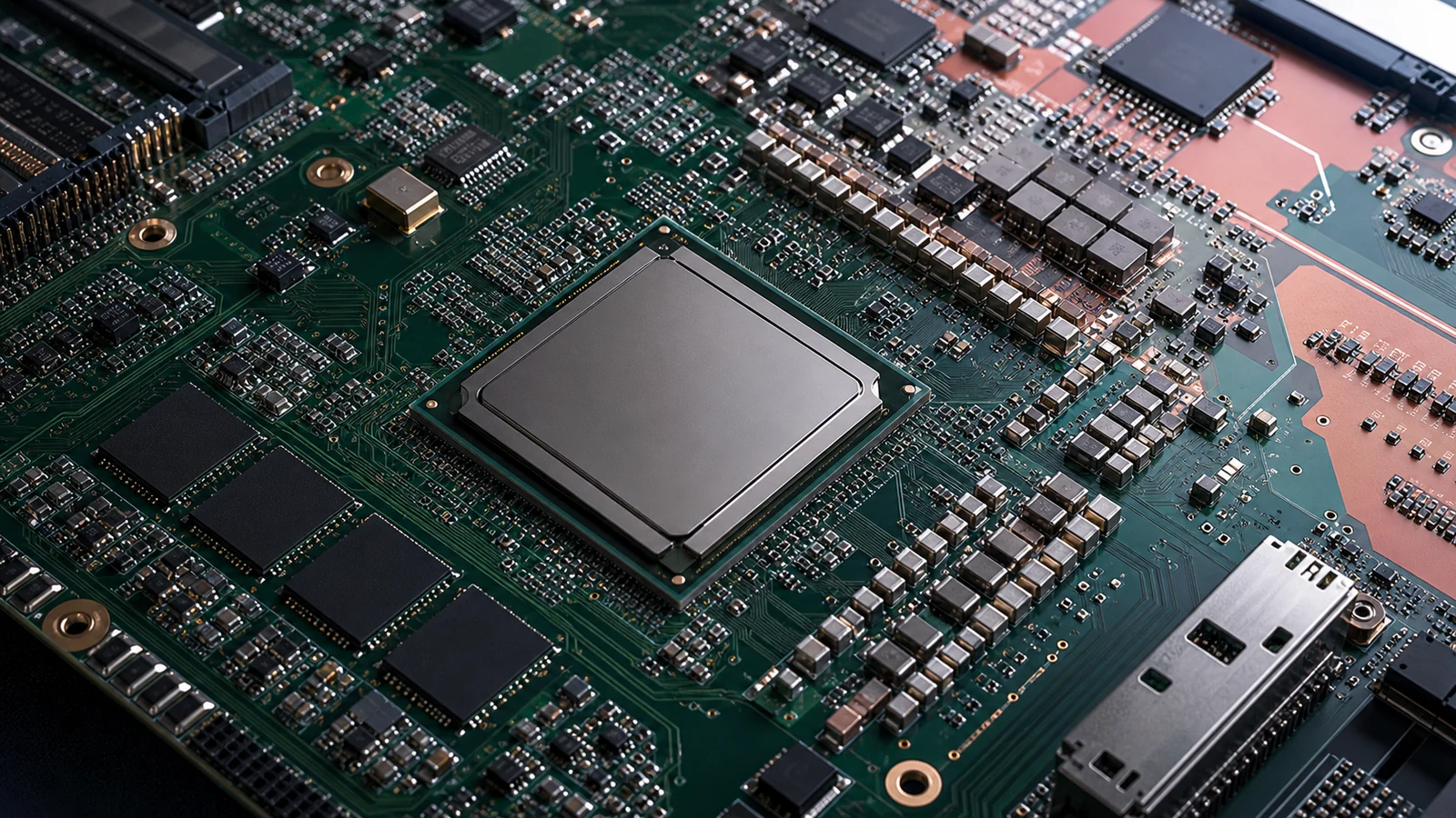
FPGA power integrity is difficult because one device may combine multiple rails, rapidly changing current demand, and a dense BGA package whose PCB and package inductance limits instantaneous current delivery. Signal escape also competes with power and ground access, while different frequency ranges rely on different parts of the PDN. Weak delivery can reduce operating margin across logic, transceivers, memory interfaces, and the wider system.
Power integrity is therefore not a final capacitor-placement exercise. The regulator, power-distribution network (PDN), package, PCB stackup, planes, vias, workload, and validation plan must be engineered as one system. Actual limits and rail requirements must come from the selected FPGA datasheet, hardware design guide, reference design, power estimator, and vendor power-integrity recommendations.
FPGA Rails, Load States, and Transient Current
Depending on the device and application, an FPGA may use core, auxiliary, I/O-bank, transceiver, memory-related, and PLL or analog-related supply domains. These rails can have different current profiles, noise sensitivity, regulator requirements, and power-up or power-down behavior. Do not transfer one vendor family’s rail architecture or sequence to another device.
Switching activity, simultaneous logic transitions, memory traffic, transceiver operation, configuration, and changing application states can alter current demand faster than a regulator can respond. Local energy storage and low-inductance delivery paths bridge the faster part of that response. A rail specification should record its allowed voltage window, static and dynamic load assumptions, source, sequence, fault behavior, and measurement point without treating every rail alike.
What Is an FPGA PDN?
An FPGA PDN is the complete network that carries energy from the voltage regulator to the device’s internal power structures. It includes the regulator output network, bulk capacitors, local decoupling, PCB planes or pours, traces, vias, package connections, and return paths. Each element contributes resistance, inductance, capacitance, or control-loop behavior, so power integrity is a system-level network problem rather than a question of capacitor count alone.
| PDN element | Main role | Common risk |
|---|---|---|
| Regulator | Supplies DC and lower-frequency energy | Control-loop interaction, thermal limits, and switching noise |
| Bulk capacitance | Supports slower load changes and regulator interaction | ESR, placement, startup, and stability effects |
| Local decoupling | Supplies faster current through a short loop | Effective capacitance and mounting inductance |
| Planes, pours, and vias | Distribute power and return current | Resistance, inductance, bottlenecks, and resonance |
| Package and die | Connect PCB delivery to internal loads | Package inductance and limited ball access |
Target Impedance and Frequency-Dependent Delivery
What is target impedance in FPGA power design?
Target impedance is a design concept that relates the voltage variation permitted on a rail to the expected change in load current. It provides a rail-specific reference for evaluating PDN impedance across the relevant frequency range, not a universal FPGA number. The useful target depends on device requirements, dynamic current, allocated ripple or droop, regulator response, package behavior, and the analysis or measurement bandwidth.
A conceptual estimate is only a starting point. Time-domain load behavior, package and regulator models, and the location where voltage limits apply all influence acceptance. Each rail needs its own assumptions and margin allocation; one target should not be applied to the whole FPGA without evidence.
Decoupling Capacitor Strategy
How should FPGA decoupling capacitors be selected?
FPGA decoupling capacitors should be selected from the required PDN response and the complete installed impedance, not nominal capacitance alone. Review voltage rating, DC-bias derating, tolerance, ESR, ESL, package size, effective capacitance, and mounting geometry. Bulk and local parts serve different portions of the load response, while interactions among capacitors, planes, vias, package, and regulator output impedance can create resonance or anti-resonance.
Bulk capacitance generally supports slower energy demand and regulator/load interaction. Local decoupling supports faster current delivery through lower-inductance loops. These are conceptual roles rather than fixed frequency boundaries. Mixing many values blindly can add impedance peaks, and substituting parts by label value alone can change the installed network.
How close should decoupling capacitors be to an FPGA?
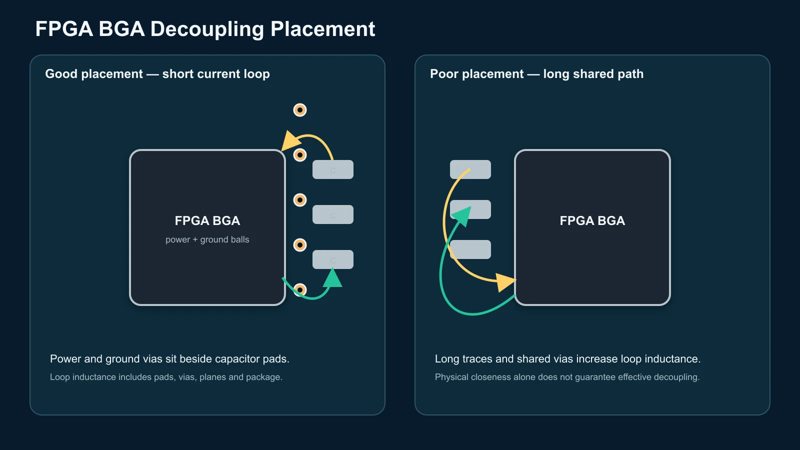
FPGA decoupling capacitors should be placed to minimize the complete inductive current loop, not to satisfy one universal package-edge distance. Effectiveness depends on capacitor package, pad-to-via geometry, power and ground via placement, plane access, package connection, and available BGA escape. A slightly farther component with direct, paired connections can outperform a closer part reached through long traces, shared vias, or plane necks.
BGA Breakout, Vias, and Ground Integrity
How do vias affect FPGA power integrity?
Vias affect FPGA power integrity through their length, placement, pairing, and contribution to the complete power-and-return loop. Properly arranged parallel current paths may reduce path impedance, but simply adding vias is not always better. Power and ground vias must reach useful planes without forcing current through congested regions, excessive plane perforation, long stubs, or shared bottlenecks around the BGA field.
Reserve power and ground access before signal escape consumes the available channels. The FPGA ball map, via technology, anti-pad field, decoupling access, and return-current structure should be reviewed together with the BGA fanout and escape-routing guidance. Via diameter, finished hole, plating, microvia construction, fill, stacking policy, and count require coordination with qualified PCB manufacturing resources rather than selection from a generic current table.
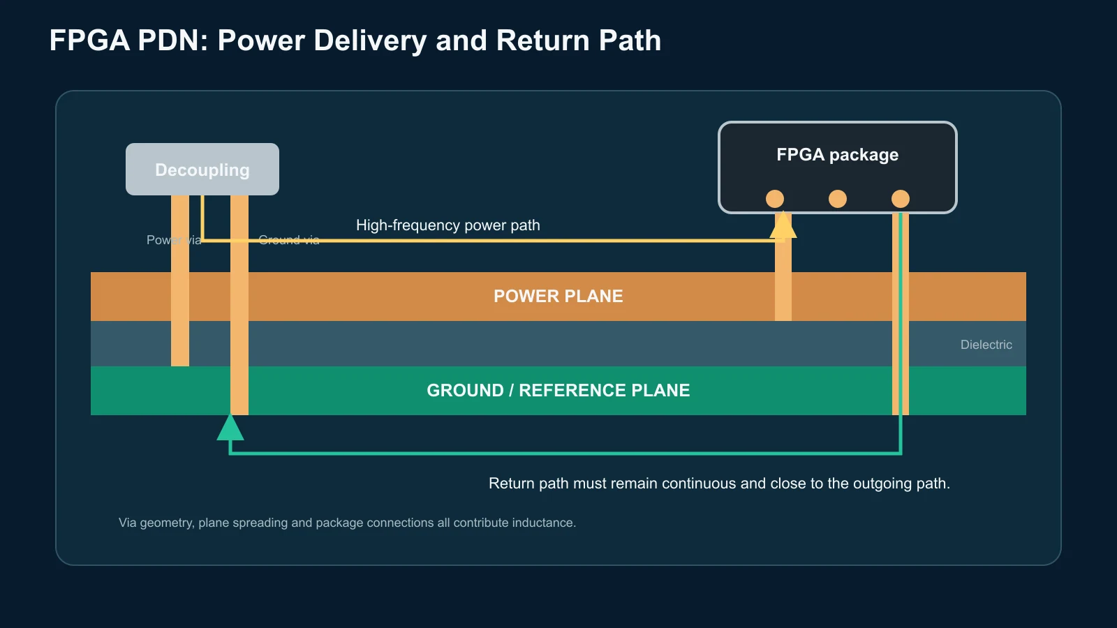
Ground is not an ideal zero-impedance reference. Ground planes, ground vias, package connections, and spreading paths carry return current and contribute inductance and current density. A low-inductance supply connection is incomplete without an equally intentional return path.
Stackup, Planes, Pours, and DC Versus AC Behavior
How does PCB stackup affect FPGA power integrity?
PCB stackup affects FPGA power integrity by defining plane geometry, coupling, via length, BGA access, and the continuity of power and signal-return paths. Closely coupled power and ground structures can reduce spreading inductance, but they do not replace local decoupling. Layer assignments must also satisfy escape routing, controlled impedance, dielectric availability, board symmetry, and reference continuity for high-speed signals.
Power may be distributed with dedicated planes, partial planes, copper pours, or wide routing structures. The appropriate choice depends on rail count, current, layer availability, routing density, voltage drop, and impedance goals. A visually broad plane can still be weak if anti-pads, slots, mounting holes, or narrow necks fragment the current path.
DC analysis addresses resistance, copper area, current density, connector loss, voltage drop, and thermal concentration. AC or transient analysis addresses inductance, capacitance, impedance versus frequency, resonance, and load-step response. A design can pass a DC-drop check and still have poor transient delivery. These relationships should remain consistent with the broader PCB layout optimization strategy.
Regulator Placement and Switching Noise
Why can switching regulators create FPGA power problems?
Switching regulators can affect FPGA power quality through output ripple, compact high-current switching loops, switching-node electric fields, magnetic coupling, and shared ground impedance. Layout should control those fields and return paths while satisfying thermal, control-loop, routing, bulk-capacitance, and load-location needs. The right placement is a system trade-off; putting every regulator as close as possible to the FPGA is not a universal rule.
Keep switching loops compact, route feedback and sense connections according to the regulator guidance, and separate or filter sensitive rails when device requirements justify it. Confirm that downstream capacitance, startup behavior, load-line response, and remote-sense location are compatible with the regulator model. Adding capacitance without checking control-loop stability can exchange one problem for another.
DDR, Transceivers, and High-Speed Interfaces
How does FPGA power integrity relate to DDR and high-speed interfaces?
FPGA power integrity and high-speed-interface margin are linked through I/O switching demand, shared reference structures, package connections, and PDN noise. Memory activity or transceiver operation can change rail current while power and ground impedance can alter the local reference environment. This interaction does not make PI the cause of every interface failure, so timing, signal integrity, and power integrity should be debugged with separate evidence.
For memory interfaces, coordinate the PDN with the DDR routing guidelines, reference-plane continuity, termination strategy, and realistic activity states. High-speed transceiver or analog-related rails may have different noise sensitivity from general digital rails; follow the selected vendor’s regulator, filtering, separation, and grounding requirements. The high-speed PCB design context is useful, but it does not replace device-specific limits.
Sequencing, Simulation, and Measurement
Some FPGA families require specific power-up, power-down, ramp, pre-bias, or differential-rail behavior. Take the actual sequence from the selected device datasheet and power-management guide. Review enable dependencies, power-good signals, reset, configuration, I/O back-powering, regulator reverse current, and discharge paths so startup and recovery remain deterministic.
PDN analysis can be useful when voltage margin is limited, the package is dense, plane access is constrained, resonances are plausible, or prototype failure would be expensive. Frequency-domain analysis can examine impedance and resonances; time-domain analysis can evaluate transient compliance; DC analysis can expose drop and current crowding. Model fidelity should match the decision rather than implying every project needs the same simulation scope.
Plan physical validation before release. Possible methods include rail probing with an appropriate low-inductance connection, oscilloscope checks, current and voltage monitoring, impedance measurement where suitable, startup and sequencing capture, and functional stress testing. Measurement point, bandwidth, loading, and probe geometry can change the observed result, so no measurement should be claimed without documented conditions.
Common FPGA Power-Integrity Mistakes
- Treating all rails alike: different domains can have different loads, sensitivity, and sequencing requirements.
- Choosing capacitors only by nominal value: bias, tolerance, ESR, ESL, package, and mounting alter installed behavior.
- Placing parts by distance alone: the complete power-and-return loop controls inductance.
- Completing signal escape first: this can remove practical power, ground, and decoupling access beneath the BGA.
- Assuming planes solve every PI problem: planes still have finite resistance, inductance, voids, and resonances.
- Adding more or larger capacitors blindly: regulator interaction and anti-resonance can make the result worse.
- Checking only DC voltage drop: acceptable resistance does not prove adequate transient response.
- Blaming all noise on the regulator: package, vias, planes, loads, and return paths also shape rail behavior.
- Copying another FPGA network: utilization, package, rail architecture, stackup, and regulator behavior may differ.
- Skipping the pre-release PDN review: late corrections can conflict with BGA escape, stackup, assembly, and manufacturing constraints.
FPGA Power Integrity Review Checklist
What should be checked before releasing an FPGA power design?
Before release, verify the selected FPGA’s rail limits, current assumptions, regulator architecture, sequencing, bulk and local decoupling, BGA power-and-ground access, stackup, DC drop, transient response, and measurement plan. Confirm vendor guidance and manufacturing constraints, then document unresolved margins. Simulation should be considered where risk justifies it, but the release decision must remain tied to traceable device requirements and review evidence.
- Device datasheet, hardware design guide, reference design, power estimator, and PI recommendations reviewed.
- Rail requirements, realistic operating states, and dynamic-load assumptions documented.
- Regulator architecture, control-loop constraints, thermal path, and sequencing checked.
- Bulk and local capacitance planned using effective installed behavior.
- Mounting loops and BGA power/ground escape reviewed before final signal fanout.
- Stackup, planes, pours, return continuity, anti-pad fields, and via construction confirmed.
- DC drop, current density, PDN impedance, resonance, and transient analysis considered at an appropriate fidelity.
- Measurement access, startup checks, workload stress cases, and acceptance evidence defined.
Engineering Context
During FPGA board development, Excel Circuit’s in-house PCB design engineers can review rail architecture, stackup, BGA breakout, decoupling, SI/PI, DDR routing, and DFM together. A representative FPGA and embedded-board case study shows why package escape, memory interfaces, and power delivery should be planned as one board-level problem.
FAQ
How many decoupling capacitors does an FPGA need?
There is no universal count. It depends on the selected FPGA and package, rail impedance target, workload, regulator response, capacitor characteristics, mounting inductance, plane structure, and available placement. Use vendor guidance as a baseline, then verify it against the project PDN.
Should every FPGA power rail use a separate plane?
No. Plane assignment depends on rail current, noise sensitivity, layer availability, return-path requirements, and stackup. Some rails can use pours or localized structures; others benefit from broad planes. Avoid plane splits that compromise high-speed return current.
Are the closest capacitors always the most effective?
Not necessarily. Electrical loop inductance is more important than straight-line distance. A slightly farther capacitor with direct power and ground via access may outperform a closer part connected through long traces or shared bottlenecks.
When is FPGA power-integrity simulation justified?
It is especially useful when voltage margins are small, current steps are large, packages are dense, plane access is restricted, anti-resonance is possible, or a failed prototype would be expensive. The scope should be chosen around specific design decisions and available model quality.
Request an FPGA Power-Architecture Review
If you are reviewing an FPGA PCB power architecture, share the FPGA package, rail requirements, regulator plan, stackup, memory or high-speed interfaces, and manufacturing constraints for engineering review.