Contents
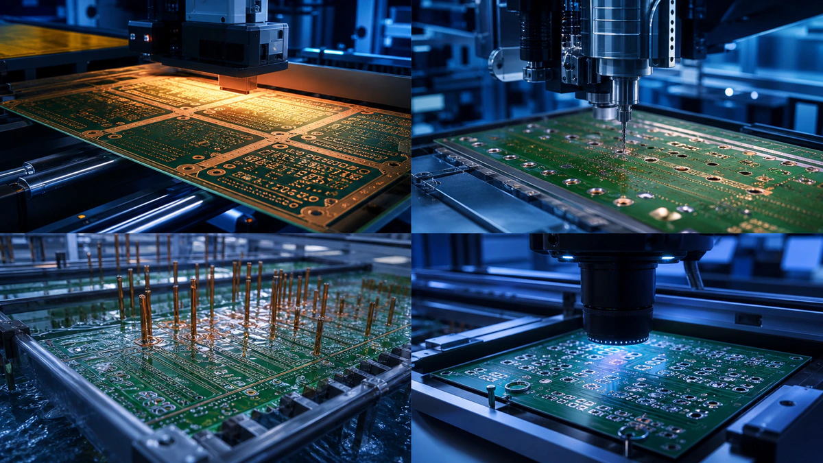
The PCB manufacturing process converts validated design data into a finished bare circuit board through imaging, etching, lamination where required, drilling, copper deposition and plating, solder-mask application, surface finishing, profiling, electrical testing and final inspection. The exact sequence varies with board construction, via technology, materials and the selected PCB fabricator, so manufacturing data must define the intended result without assuming one universal process flow.
This engineering guide explains the major fabrication stages, the quality risks at each stage and what designers should confirm before release. It covers bare PCB fabrication—not component placement, solder-paste inspection, reflow, X-ray or other PCBA assembly operations.
What Are the Main Stages of PCB Manufacturing?
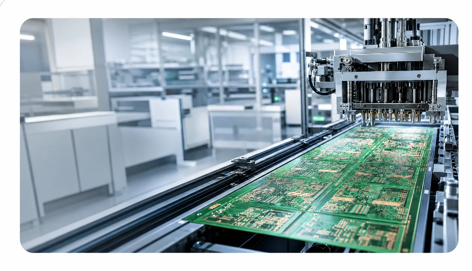
The main stages are manufacturing-data review, image transfer, copper etching, multilayer lamination where applicable, drilling and hole preparation, copper metallization and plating, outer-layer processing, solder mask, surface finish, legend, profiling, electrical test and final inspection. Conventional standard PCB manufacturing may omit multilayer operations for single- and double-sided boards, while HDI, blind/buried-via and special-material boards can require additional or repeated cycles. These manufacturing stages are easier to control when PCB design fundamentals for manufacturability are correct. Those repeated cycles are covered under advanced PCB manufacturing technologies.
| Process stage | Purpose | Key engineering risk |
|---|---|---|
| CAM and data review | Translate released files into a manufacturable job | Missing or conflicting fabrication instructions |
| Imaging and etching | Create the required copper pattern | Trace geometry, spacing and registration variation |
| Layup and lamination | Build the multilayer construction | Layer alignment, resin flow and dielectric consistency |
| Drilling and metallization | Create and connect holes and vias | Hole location, wall preparation and plating continuity |
| Solder mask and finish | Protect copper and create solderable surfaces | Mask registration and finish suitability |
| Electrical test and inspection | Verify connectivity and workmanship | Opens, shorts, dimensional defects and documentation mismatch |
1. Manufacturing Data Review and CAM Preparation
CAM review is required before PCB fabrication because the released design files must be checked for completeness, consistency and compatibility with the selected process capability. The review does not redesign the circuit. It identifies ambiguous layer order, missing drill data, conflicting outlines, unclear via instructions, unsupported materials or other issues that should be resolved before irreversible fabrication work begins.
A release package may include Gerber or ODB++ data where applicable, NC drill files, the board outline, stackup, fabrication drawing, impedance requirements, material and copper-weight requirements, surface finish and special instructions for blind/buried vias, microvias or via-in-pad. The deeper Gerber file checklist for PCB manufacturing explains how to verify the production-file package without duplicating it here.

2. Inner-Layer Imaging, Etching and Inspection
Photoresist and Pattern Imaging
For multilayer boards, the inner-layer copper pattern is transferred to copper-clad core material using photoresist and controlled imaging. Fabricators may use phototools or direct-imaging equipment depending on their process. The important engineering result is accurate transfer of the intended copper geometry and registration features—not one mandatory imaging method.

Copper Etching
Etching removes unwanted copper while the protected areas form traces, pads and planes. Etch control matters because the finished geometry—not merely the nominal CAD width—affects clearance, current paths and controlled-impedance behavior. Copper thickness, feature density and process conditions influence the result, so universal trace/space rules should not be inferred from this overview.
Inner-Layer AOI
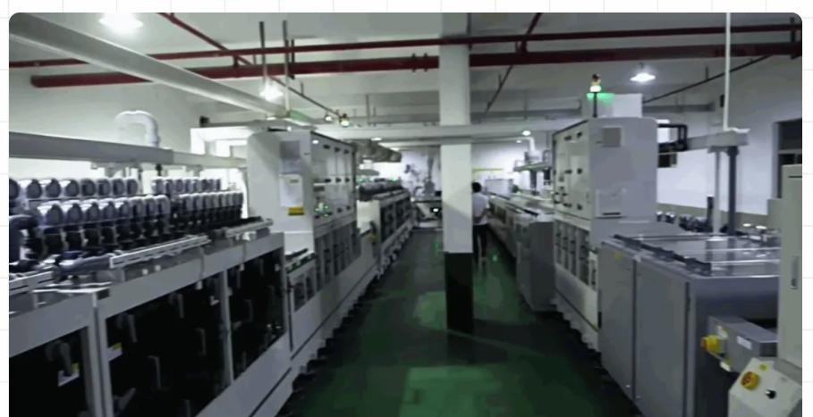
Automatic optical inspection can compare etched inner layers with the manufacturing data to identify pattern defects before those layers are buried inside a multilayer stack. Registration and etch quality influence spacing, conductor shape, impedance consistency and yield. AOI is a bare-board fabrication control; it should not be confused with assembly AOI used after components are placed and soldered.

3. Multilayer Layup and Lamination
A multilayer PCB is laminated by aligning etched cores with prepreg and copper foil in the specified layer sequence, then applying a controlled press cycle so the resin flows, bonds and cures into a consolidated structure. Press temperature, pressure and timing depend on the selected material system, board construction and fabricator process; they are not universal design values. For a layer-by-layer explanation, review PCB structure and layer functions.
Stackup matters during manufacturing because it defines the physical relationship among copper layers, dielectric materials, dielectric thicknesses and finished board thickness. Those choices affect impedance, reference-plane coupling, routing structure, via feasibility, resin behavior and mechanical balance. The production stackup should therefore be confirmed with the selected fabricator rather than treated as a decorative CAD note. See the PCB stackup design guide for the engineering decisions behind that specification.

4. Drilling, Desmear and Via Formation
PCB holes and vias are formed with processes selected for their structure: through holes are commonly mechanically drilled, while many microvias are laser drilled; blind and buried vias require layer-specific processing and may be created during sequential build-up. After drilling, hole walls are cleaned and desmeared as required so resin residue does not prevent reliable metallization.
Through, blind, buried and microvia structures are not interchangeable and do not all follow one drilling sequence. The released drawing and drill data should identify hole function, plating status and layer pairs. HDI designs may add laser-drilled microvias, repeated imaging and lamination cycles, copper filling or via-in-pad processing. The Via-in-Pad PCB Design Guide covers VIPPO and filling considerations in more detail.

5. Electroless Copper and Electroplating
After suitable hole-wall preparation, a thin electroless-copper layer can create a conductive path over the nonconductive hole wall; electroplating then builds copper on the hole walls and selected board surfaces according to the fabrication process. The resulting metallization creates electrical continuity between layers and contributes to via reliability and current-carrying capability.
Plating quality depends on preparation, chemistry control, current distribution and geometry. Designers should specify the electrical and structural requirement, while the selected fabricator defines a capable process. This guide intentionally does not prescribe a universal copper thickness, aspect ratio or minimum drill size.

6. Outer-Layer Imaging and Etching
Outer-layer circuitry is imaged and processed after the drilled structure has been prepared for metallization. The exact pattern-plating and etching sequence can differ by fabricator and board technology. Finished outer-layer geometry must satisfy spacing, pad, annular-ring and impedance requirements after the relevant copper and finish processes—not only at the image-transfer stage.
7. Solder Mask, Legend and Surface Finish
Solder Mask
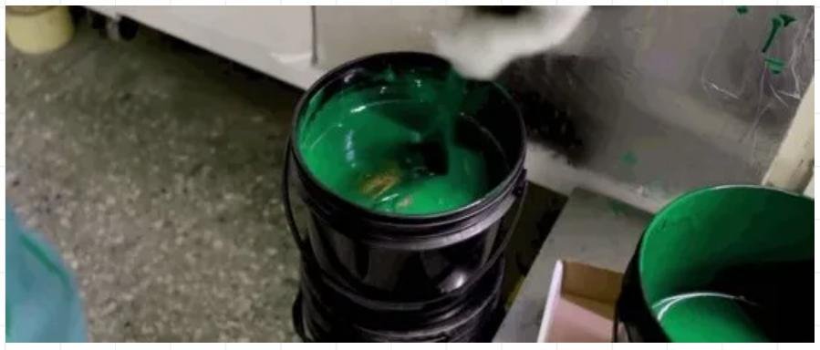
Solder mask protects selected copper surfaces, helps control solder during assembly and defines openings around pads and other exposed features. Application, imaging and curing must maintain registration to the copper pattern. Mask clearances and dams should be reviewed against the selected process rather than assumed from generic values.
Legend or Silkscreen
Legend can add component references, polarity marks, identifiers and assembly information where required. It should remain readable without covering pads, test features or exposed copper. Legend is useful documentation, but it does not replace controlled fabrication and assembly drawings.
Surface Finish
Surface finish protects exposed copper and creates solderable or contact surfaces. HASL, ENIG, ENEPIG and OSP are common options, but no finish is universally best. Selection depends on component pitch, assembly process, contact function, shelf-life needs, application environment, cost and the capabilities of the selected manufacturing resource.

8. Controlled Impedance During Fabrication
Controlled impedance is managed by coordinating the electrical target with the production stackup and the selected fabricator’s achievable geometry. Dielectric properties, dielectric thickness, finished copper thickness, trace width, spacing, copper roughness and process compensation can all affect the result. A generic trace width cannot guarantee a target impedance across different materials and constructions.
The fabrication drawing should identify controlled nets or structures, target values and any test-coupon requirement. The fabricator can then review or adjust production geometry while preserving the electrical objective. The focused guide on designing a 50-ohm PCB trace explains why the complete transmission-line structure matters.
9. Profiling, Routing and Final Dimensions
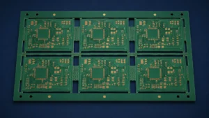
Individual boards or production panels are profiled by routing, scoring or another suitable method. The board outline, slots, cutouts, edge features and dimensional requirements must be unambiguous in the release package. Profiling choices also affect panel handling, edge quality and how boards are separated before or after assembly.

10. Bare-Board Electrical Test and Inspection
Finished bare PCBs are commonly electrically tested for opens, shorts and unintended connectivity by flying-probe or fixture-based methods selected for the job. Flying probe can be practical for prototypes and lower volumes, while dedicated fixtures can improve throughput for suitable production volumes. Test coverage and method should be confirmed with the selected fabricator rather than assumed to be identical for every order.
Quality control may also include visual inspection, dimensional checks, AOI of etched layers, microsection analysis where required and impedance-coupon testing when specified. These are bare-PCB fabrication controls. Solder-paste inspection, component-placement AOI, X-ray of assembled BGAs and functional PCBA testing belong to the assembly/test flow and should not be conflated with bare-board inspection.

Why DFM Must Be Completed Before Fabrication
DFM should be completed before fabrication because the design rules, stackup, hole structures and documentation must match an achievable manufacturing process before material is committed. A useful review checks trace/space, annular ring, drill-to-copper clearance, via structure, copper distribution, solder-mask clearance, board-edge clearance, material availability, stackup and impedance feasibility.
DFM does not mean applying one factory’s generic limits to every design. It means resolving the intended performance against the selected fabricator’s qualified capability and documenting the agreed construction. See the full PCB design for manufacturability guidelines for a deeper review framework.
What Engineers Should Confirm Before Releasing Fabrication Data
- Gerber or ODB++ data is complete and matches the approved revision.
- NC drill data identifies plated, non-plated and layer-specific holes correctly.
- The board outline, slots and cutouts are unambiguous.
- The production stackup and finished thickness are confirmed.
- Material system, copper weight and surface finish are specified.
- Controlled-impedance requirements and any coupon instructions are defined.
- Through, blind, buried, microvia and via-in-pad structures are identified.
- Fabrication drawings and notes agree with the electronic data.
- Special inspection, testing, marking and packaging requirements are documented.
PCB Manufacturing Support from Design Through Assembly
Excel Circuit supports PCB projects through design review, DFM, fabrication-data review and stackup/impedance coordination, with PCB manufacturing services supported by qualified PCB manufacturing resources. When assembly is required, the project can continue through component sourcing and in-house SMT assembly. This coordinated path keeps design intent, fabrication requirements and assembly inputs aligned.
Prepare Your PCB for Manufacturing Review
If your PCB is ready for fabrication, share the Gerber or ODB++ data, drill files, stackup, impedance requirements and fabrication notes for engineering review and manufacturing coordination.