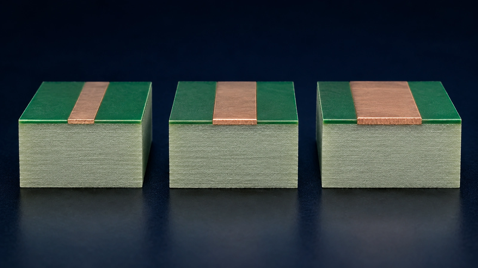
PCB copper weight is the mass of copper per unit area, commonly expressed in oz/ft². It corresponds approximately to a physical foil thickness: 1 oz is about 35 μm and 2 oz about 70 μm. Increasing copper thickness can improve conductor current and heat-spreading capability, but it also changes etching, minimum trace geometry, spacing and fabrication complexity. Heavier copper is useful when it solves a defined constraint; it is not automatically the better board specification.
Choose copper by layer, using the electrical load, available routing area and manufacturing process together. A power layer and a fine-pitch signal layer may need different copper thicknesses. Confirm whether the quoted value describes starting foil or finished copper before comparing options.
| Copper weight | Approximate nominal thickness | Typical design context | Main advantage | Manufacturing consideration |
|---|---|---|---|---|
| 1 oz | 35 μm | General electronics and suitable power paths | Common starting point with routing flexibility | Geometry still needs process confirmation |
| 2 oz | 70 μm | Higher-current or heat-spreading layers | Greater conductor cross-section | Width and spacing allowances may increase |
| Heavy copper | Specify the actual thickness | Power conversion and demanding power distribution | More copper within a given routing width | Etching, lamination and feature compatibility need review |
What Does PCB Copper Weight Mean?
Copper weight describes an area-based quantity, not the weight of copper on the entire PCB. The familiar ounce values are convenient shorthand for nominal foil thickness. Rogers’ material selector lists 1 oz as 35 μm and 2 oz as 70 μm. These approximate conversions do not establish a finished-board tolerance.
Base copper is the starting foil on the laminate. Plated copper is copper added during processing, including hole-wall metallization and, depending on the process, outer-layer conductors. Finished copper is the copper remaining in the completed feature after the relevant processing. Surface finish is a separate specification; its presence does not turn a starting-foil value into a guaranteed conductor thickness.
Inner layers commonly obtain their conductor thickness from the starting foil and subsequent processing. Outer layers may also receive copper plating. Consequently, “2 oz copper” without a layer assignment or a base-versus-finished definition leaves room for different interpretations. Specify the required finished condition and agreed acceptance basis where it matters electrically, rather than assuming every layer receives the same treatment.
When Is 1 oz Copper Sufficient?
1 oz copper is a practical choice for many control, digital, instrumentation and general-purpose boards. It can also serve power circuits when trace width, copper area, current waveform and cooling provide adequate electrical and thermal margin.
Its value is manufacturing and layout flexibility. Fine-pitch component escapes and close conductor features may be easier to reconcile with a thinner copper process than with heavy copper. That does not guarantee a particular minimum feature size: the material, layer position and fabrication process still matter.
Before increasing thickness, check whether a modest routing change removes the limitation. A wider short connection or a better current distribution path may address voltage drop without changing copper on every layer. Validate the resulting design under its actual load; nominal copper weight alone cannot establish that the path is adequate.
When Does 2 oz Copper Help?
2 oz copper offers a larger conductor cross-section than 1 oz at the same nominal width. Designers may select it for power distribution, motor-control sections, converters or layers that spread heat from concentrated sources.
The electrical benefit must be evaluated with the complete path. A wider copper region does little for a narrow neck at a connector or an undersized layer transition. More copper can spread heat, but the board still needs a route for that heat to leave the assembly and enclosure.
The trade-off is reduced freedom in some geometries and an altered process requirement. Ask whether existing pad clearances, trace spaces and fine-pitch escapes remain manufacturable. If only power layers need greater thickness, compare that construction with an all-layer change. A copper revision made after routing can require another geometry and impedance review.
What Changes With Heavy Copper?
Heavy copper describes a construction using substantially thicker copper for demanding electrical or thermal functions. Suppliers use different naming conventions, so the label should never replace the actual layer-by-layer thickness specification.
Power conversion, industrial power distribution and some battery-related electronics can justify this approach when available board area limits conductor width. The thicker features may support useful cross-section within the outline, but connectors, terminals, protection devices and vias remain possible bottlenecks.
Fabrication needs closer coordination because thick copper features affect etching and the amount of resin needed to fill spaces during lamination. Copper distribution and combinations of dense signal features with broad power areas also influence the practical construction. Do not assume a heavy-copper process available for one stackup transfers unchanged to another material or layer count.
Copper Weight and Current Capacity
Current capacity depends on the conductor’s geometry and thermal environment, not copper weight alone. Thickness contributes to cross-section, while heat generation and heat removal determine the operating temperature.
- Width and actual thickness: review the narrowest sections, not only the main pour.
- Allowable temperature rise: identify the thermal margin available to the board and nearby components.
- Ambient and enclosure conditions: account for the real operating environment and airflow.
- Layer position and adjacent copper: internal and external conductors have different heat-transfer conditions; nearby copper can change spreading.
- Load profile: distinguish continuous load, duty cycle, transients and startup conditions.
- Voltage drop: a path may meet a temperature objective yet fail its electrical budget.
Use a suitable engineering model and verify its assumptions against the intended construction. A universal “trace width equals current” table would conceal those assumptions. The high-current layout and current-path review covers broader routing, return-path and thermal decisions; this guide focuses on choosing and specifying the copper.
How Copper Weight Affects Trace Width and Spacing
Thicker copper can require greater manufacturing allowances because the etch process must remove more copper while preserving the intended conductor profile. The finished conductor is not necessarily a perfect rectangular cross-section matching the artwork.
Minimum width and spacing therefore need confirmation for the selected copper thickness and layer process. A rule accepted for thin signal copper should not be copied unchanged onto a heavy-copper layer. Review fine-pitch pads, narrow gaps, isolated copper islands and neck-downs before releasing the drawing.
Copper distribution matters as well. Large differences in copper coverage can complicate processing and board balance. Manufacturing compensation or added copper features should be reviewed for their electrical implications, especially near controlled-impedance structures. Agree on acceptable adjustments instead of treating every fabrication change as electrically neutral.
Keep electrical spacing requirements separate from manufacturing spacing. A process may be able to etch a gap that is still unsuitable for the voltage or insulation requirement. Copper thickness selection must satisfy both constraints.
Check Vias Wherever Current Changes Layers
Via current passes through the conductive hole-wall structure and its connections to the layers. Increasing planar copper thickness does not automatically increase via-barrel plating or guarantee adequate current transfer.
Review finished hole size, plating requirements, barrel length, pad connections and the arrangement of parallel vias. Current sharing depends on how the copper approaches and leaves the array; closely grouped vias should not simply be assigned identical independent current ratings and added together.
For thermal transfer, also consider the path beyond the via field. An array can spread heat to another layer without providing an effective exit to the environment. Specify the electrical and thermal purpose so the fabricator and design team review the right features. The companion PCB via structure selection guide explains the available inter-layer constructions.
Coordinate Copper Thickness With the Stackup
Copper thickness forms part of the stackup and influences conductor geometry, dielectric spacing and controlled impedance. Changing it can alter both the electrical model and the construction needed to achieve the total board thickness.
Record inner and outer copper separately. Check the relationship between etched copper features, prepreg selection and resin fill rather than viewing copper as an isolated purchasing option. Review copper balance across the construction with the fabricator; a nominally symmetric layer count does not by itself guarantee balanced copper distribution.
If impedance matters, use the agreed finished geometry and material construction for the calculation. Reconfirm trace dimensions after any approved copper or dielectric change. The PCB stackup planning guide addresses layer functions, reference planes and material coordination in greater depth.
What Drives the Cost of Heavier Copper?
Copper-related cost includes material and processing consequences, not only the additional metal. More demanding etching, revised lamination conditions and reduced compatibility with small features can narrow the available manufacturing process options.
Panel planning and yield may also be affected by the particular design. A board that combines heavy copper with dense geometry can present a different challenge from a spacious power board using the same nominal weight. Production volume and repeatability expectations influence which process is commercially practical.
Compare quotations against the same finished requirements, layer assignments and acceptance conditions. A cheaper quote using different starting foil or a different interpretation of finished copper is not an equivalent offer. Avoid applying a generic percentage premium to all 2 oz or heavy-copper boards.
How to Choose Copper Weight Before Release
Start with the limiting requirement and select the least complicated construction that meets it with verified margin.
- Map the demand. Identify power nets, continuous and peak loads, permitted voltage drop and temperature rise.
- Check available geometry. Review routing width, bottlenecks, connector entries and the space remaining around fine-pitch features.
- Assign copper by layer. Compare suitable 1 oz, 2 oz or heavier options within the intended layer count and board thickness.
- Review transitions and heat paths. Confirm that vias and component interfaces do not negate the conductor improvement.
- Obtain a fabrication review. Agree on achievable geometry, finished copper interpretation, stackup and impedance implications.
- Validate and release one definition. Record the accepted construction, assumptions and evidence in the controlled fabrication package.
For example, a dense controller with one high-current section may benefit from targeted power-layer changes rather than heavier copper everywhere. A compact power board with little routing width may need a different construction. Neither example determines the final choice without the load and process review.
Information Required From the Customer
Provide the data that connects the electrical requirement with a manufacturable construction:
- Gerber or ODB++ data and the relevant fabrication drawing revision.
- Proposed stackup, layer count and finished board thickness.
- Copper requirements by layer, identifying base or finished copper where specified.
- Current requirements, power-net locations and relevant duty-cycle information.
- Allowable temperature rise, thermal environment and voltage-drop constraints.
- Controlled-impedance requirements and geometry restrictions.
- Via or plating requirements that influence the power path.
- Build quantity and expected production volume for process planning.
Use the production-file checklist to keep the drawing, stackup and manufacturing data consistent. Mark unresolved copper assumptions for review instead of burying them in an informal email.
Review Copper Requirements Before Fabrication
Excel Circuit connects in-house PCB design engineering with qualified PCB manufacturing resources and production-readiness support. Copper selection should be settled alongside the geometry and stackup, before fabrication data is released.
Send your Gerber data, stackup and copper requirements for a manufacturability review. Include power-net loads and thermal constraints so the review can address the actual conductor requirement. Submit your copper and fabrication requirements.