Contents
What Is PCB Layout Engineering?
PCB layout engineering converts an approved schematic and design constraints into a manufacturable physical board definition. The work covers component placement, stackup coordination, routing, return-current paths, power distribution, thermal planning, design-rule implementation, and production-data verification. A completed layout must satisfy electrical, mechanical, fabrication, assembly, and test requirements at the same time.
Excel Circuit provides PCB design and layout support for prototypes and production-oriented hardware, including multilayer, high-speed, RF, FPGA, embedded, analog, mixed-signal, and power-electronics projects. Layout scope is defined from the actual files and constraints rather than from board size alone. Those scope choices are the main PCB layout cost drivers.
What Inputs Are Required Before Layout Starts?
A reliable PCB layout begins with a controlled schematic, component data, mechanical constraints, and clearly identified electrical rules. Missing or changing inputs create placement and routing rework, so assumptions should be recorded before the layout baseline is approved.
- Current schematic and design revision
- BOM with manufacturer part numbers and package information
- Verified symbols, footprints, and pin assignments where available
- Board outline, mounting holes, connectors, keepouts, and height limits
- High-speed interfaces, impedance targets, timing constraints, and clocks
- Power rails, current requirements, sensitive analog or RF sections, and thermal limits
- Target stackup, materials, via structures, and qualified fabrication rules
- Assembly, inspection, test-access, and deliverable requirements
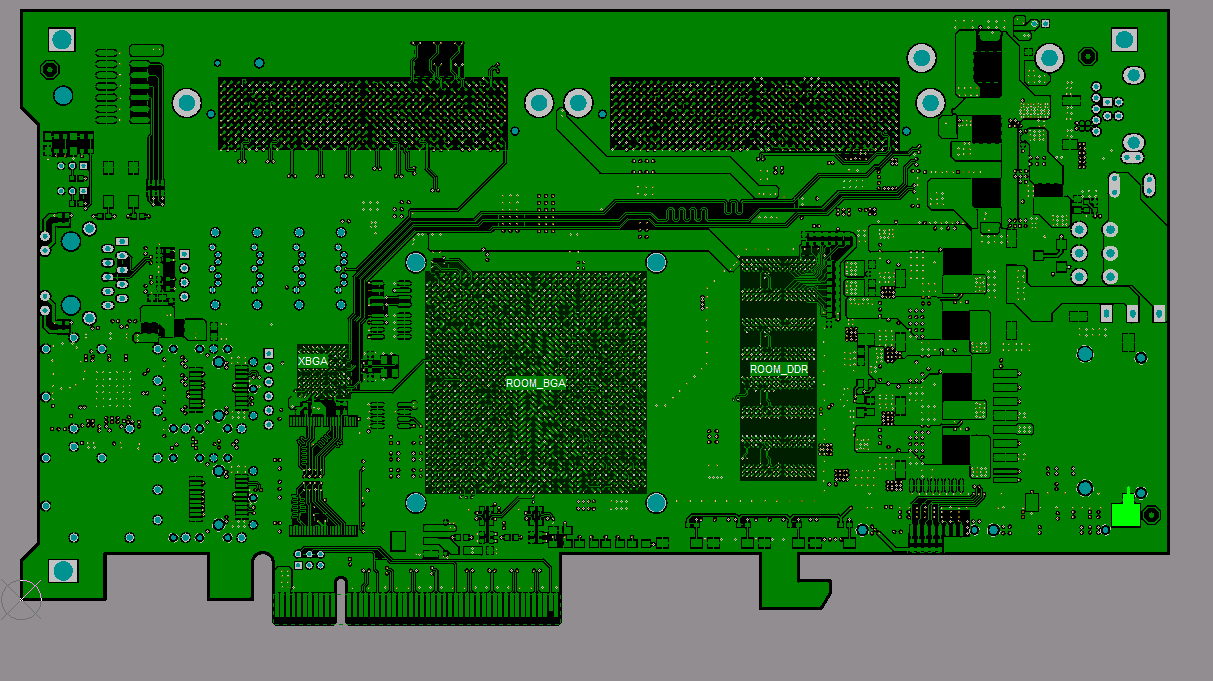
For FPGA and dense BGA designs, package pin assignment, escape planning, DDR topology, transceiver requirements, and rail sequencing should be reviewed early. Mechanical models or enclosure data are also important when connector positions and component heights are fixed.
PCB Layout Engineering Workflow
1. Requirement and schematic review
The engineer checks connectivity, interfaces, component packages, power architecture, critical nets, mechanical restrictions, and open decisions. This review defines the layout scope and identifies information that must be resolved before detailed routing.
2. Stackup and design-rule planning
The PCB stackup assigns signal layers, reference planes, dielectric construction, copper weights, and via options. Controlled-impedance geometry must be coordinated with the intended fabricator because finished copper and dielectric properties determine the manufactured result. See the PCB stackup design guide for the electrical and manufacturing relationships.
3. Component placement
Placement establishes signal paths, power loops, return-current continuity, routing channels, thermal paths, assembly access, and mechanical fit. Critical components are positioned from functional relationships rather than from visual symmetry.
4. Critical routing
Critical nets are routed according to topology, impedance, reference-plane, spacing, skew, current, and transition requirements. Differential pairs do not become correct merely because their visible lengths match; the complete channel, package delay, via transitions, and reference continuity must satisfy the applicable interface constraints.
5. Power, ground, thermal, and EMI review
Power distribution connects sources, loads, planes, decoupling capacitors, vias, and return paths as one network. High-current transitions and neck-downs are checked for voltage drop and heating. Sensitive analog and RF areas are evaluated for coupling, while switching loops and plane discontinuities are reviewed for EMI risk.
6. DFM, DFA, and release verification
The released design is checked against fabrication and assembly capability, including trace and spacing rules, drills, annular rings, mask clearances, component spacing, polarity, test access, and documentation. This release gate closes the enterprise PCB design process. A DFM, DFA and DFT review aligns fabrication, assembly and test readiness. A PCB design review checklist keeps the verification traceable. The PCB design for manufacturability guide explains the pre-release checks in detail.
How Layout Requirements Change by Project Type
| Project type | Primary layout concerns | Related engineering page |
|---|---|---|
| High-speed digital | Topology, controlled impedance, timing, return paths, via transitions, and crosstalk | High-speed PCB design |
| FPGA and embedded | BGA escape, DDR, transceivers, clocks, multiple rails, and PDN behavior | Embedded and FPGA PCB design guide |
| RF and wireless | Transmission-line geometry, grounding, isolation, loss, launches, and antenna clearance | RF PCB design guide |
| Power electronics | Current paths, copper distribution, switching loops, creepage, clearance, and thermal design | High-current PCB layout |
| HDI and fine-pitch BGA | Escape density, microvias, via-in-pad, build-up layers, and fabricator capability | BGA fanout guide |
What Should Be Verified Before PCB Release?
- The schematic, layout, BOM, and mechanical data use the same approved revision.
- Critical interfaces follow documented topology, impedance, spacing, and timing rules.
- Every signal transition has an appropriate reference-current path.
- Power and ground access is not compromised by BGA escape or routing congestion.
- High-current paths include pads, vias, connectors, planes, and neck-downs in the review.
- Board outline, holes, keepouts, component heights, and connector positions match mechanical data.
- Fabrication and assembly outputs are regenerated from the final approved database.
- Gerber or ODB++ data, drill files, pick-and-place data, and drawings are viewed and cross-checked before release.
PCB Layout Deliverables
Deliverables depend on the agreed EDA environment and project scope. They may include editable source files, fabrication data, NC drill files, assembly drawings, pick-and-place data, BOM outputs, stackup and impedance notes, 3D or mechanical exports, and design-review records.
Request a PCB Layout Engineering Review
Send the available schematic, BOM, board outline, interface requirements, and target schedule for an engineering review. Excel Circuit can coordinate PCB layout, DFM/DFA, qualified fabrication resources, component sourcing, and in-house SMT assembly within one project workflow. An NDA can be arranged before confidential design files are reviewed.