Contents
BGA fanout and escape routing is the process of moving signal, power, and ground connections from the BGA ball field into routable PCB channels using surface traces, through vias, blind vias, microvias, or via-in-pad structures as appropriate. Fanout creates access from the pad field to vias and routing channels, while escape routing carries those connections beyond the dense package area. The strategy depends on package pitch, ball map, stackup, routing density, high-speed constraints, and fabrication capability.
Table of Contents
- What Is BGA Fanout and Escape Routing?
- What Determines the BGA Fanout Strategy?
- Dog-Bone Fanout vs Via-in-Pad
- Through-Via, Blind-Via and Microvia Strategies
- How to Plan Escape Routing by BGA Density
- BGA Fanout for High-Speed Interfaces
- Power and Ground Escape Planning
- BGA Fanout and PCB Stackup
- Common BGA Fanout Routing Mistakes
- How to Check BGA Escape Routing Before Release
- When HDI Is Useful for BGA Fanout
- Engineering Checklist
- FAQ
- Working on a Fine-Pitch BGA or FPGA Board?
What Is BGA Fanout and Escape Routing?
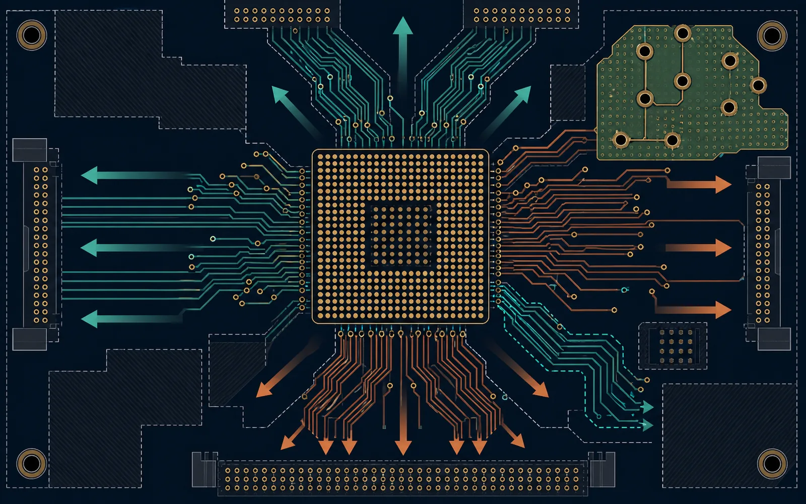
Fanout focuses on bringing BGA ball connections from the pad field to vias and usable routing channels. Escape routing continues those connections out of the congested package area so they can be routed across the board. The terms are often used together, but they emphasize different stages of the same breakout-planning process.
In PCB layout services, a successful fanout strategy creates enough routing channels while protecting reference continuity, power delivery, assembly yield, and fabrication reliability. Dog-bone escapes, through vias, blind vias, microvias, and via-in-pad each solve different density problems. The correct option depends on the actual package, net assignment, layer stack, board thickness, material system, and qualified manufacturing process. A related HDI & Fine-Pitch BGA Engineering Example shows how these decisions are coordinated.
- Analyze the BGA map before placement is frozen.
- Classify pins by signal, power, ground, and routing priority.
- Select fanout and stackup together.
- Use the least complex via technology that meets escape and electrical requirements.
- Confirm the proposed geometry with fabrication and assembly teams.
What Determines the BGA Fanout Strategy?
BGA fanout strategy is determined by package pitch and land geometry, ball-map organization, the depth and distribution of signal rows, available routing channels, stackup and reference needs, via architecture, and the selected fabricator’s capability. Pin count alone is not a reliable measure of breakout difficulty; two packages with similar counts can require different fanout methods because their pin locations, destinations, and board constraints differ.
The engineering problem is to move hundreds or thousands of nets from a confined pad field into usable routing layers without creating unmanufacturable clearances, excessive via stubs, broken return paths, weak power distribution, solder-wicking risk, or unnecessary sequential lamination. Pitch alone does not determine the solution. Package geometry, net organization, the proposed stackup, and the selected supplier’s qualified process must be evaluated as one system.
BGA Pitch
BGA pitch affects the room available for pad escape, neck-down traces, vias, antipads, and routing channels, but it does not prescribe one via type or layer count. As pitch becomes finer, conventional dog-bone and through-via approaches can become constrained by land geometry and fabrication limits, so blind microvias or via-in-pad may become appropriate. The decision remains package-, stackup-, and fabricator-specific.
Pitch sets the geometric starting point, but it is not a complete routing rule. It affects the space between lands, the room available for neck-down traces, and whether a via can be placed between pads or must be moved into a pad. However, two packages with the same pitch can require different strategies because their ball diameters, solder-mask definitions, row depths, depopulated areas, and pin assignments differ. Use the component manufacturer’s land-pattern guidance, then test it against actual fabrication and assembly constraints. Avoid mapping a pitch to one mandatory via type or layer count.
Ball Map and Pin Distribution
The ball map determines where routing demand appears. Peripheral low-speed pins may leave the package on outer-layer traces, while deeply nested signals require access to internal channels. Power and ground islands, differential pairs, memory byte lanes, clock groups, and I/O banks can either simplify or obstruct escape paths. Classify the verified pin map before routing, identify legal pin swaps, and consider whether the device vendor permits bank-aware reassignment. For programmable logic, Embedded & FPGA PCB Design provides broader context for pin planning and package integration. Pin count by itself does not measure escape difficulty.
Stackup and Routing Layers
Routing layers determine how many usable paths are available beneath and around the package, but a nominal layer count is not the same as real capacity. Plane assignments, reference requirements, antipads, copper weights, dielectric construction, and routing direction all consume or restrict space. Define which layers can accept BGA escapes, which planes provide the return path, and where transitions occur. A proposed via architecture that cannot be built within the intended stackup is not a viable fanout plan.
Fabrication Capability
The PCB fabricator should be involved before the BGA fanout and stackup are locked. Confirm achievable trace and space, mechanical-drill and microvia capability, via-in-pad processing, copper and plating rules, registration tolerance, stackup construction, and impedance requirements for the intended build. Final geometry must be validated against the selected fabricator’s actual rules; design requirements can be coordinated with qualified PCB manufacturing resources.
Minimum trace and space, mechanical and laser drilling, registration, annular-ring control, dielectric thickness, via fill, planarization, plating, and sequential-lamination capability vary by supplier and construction. Obtain stackup and design-rule input from the selected fabricator before finalizing the breakout. Capabilities stated on a generic technology table may carry conditions related to panel size, copper thickness, material, yield, or inspection. Use qualified limits and appropriate production margins rather than treating an advertised minimum as the default design rule.
Dog-Bone Fanout vs Via-in-Pad
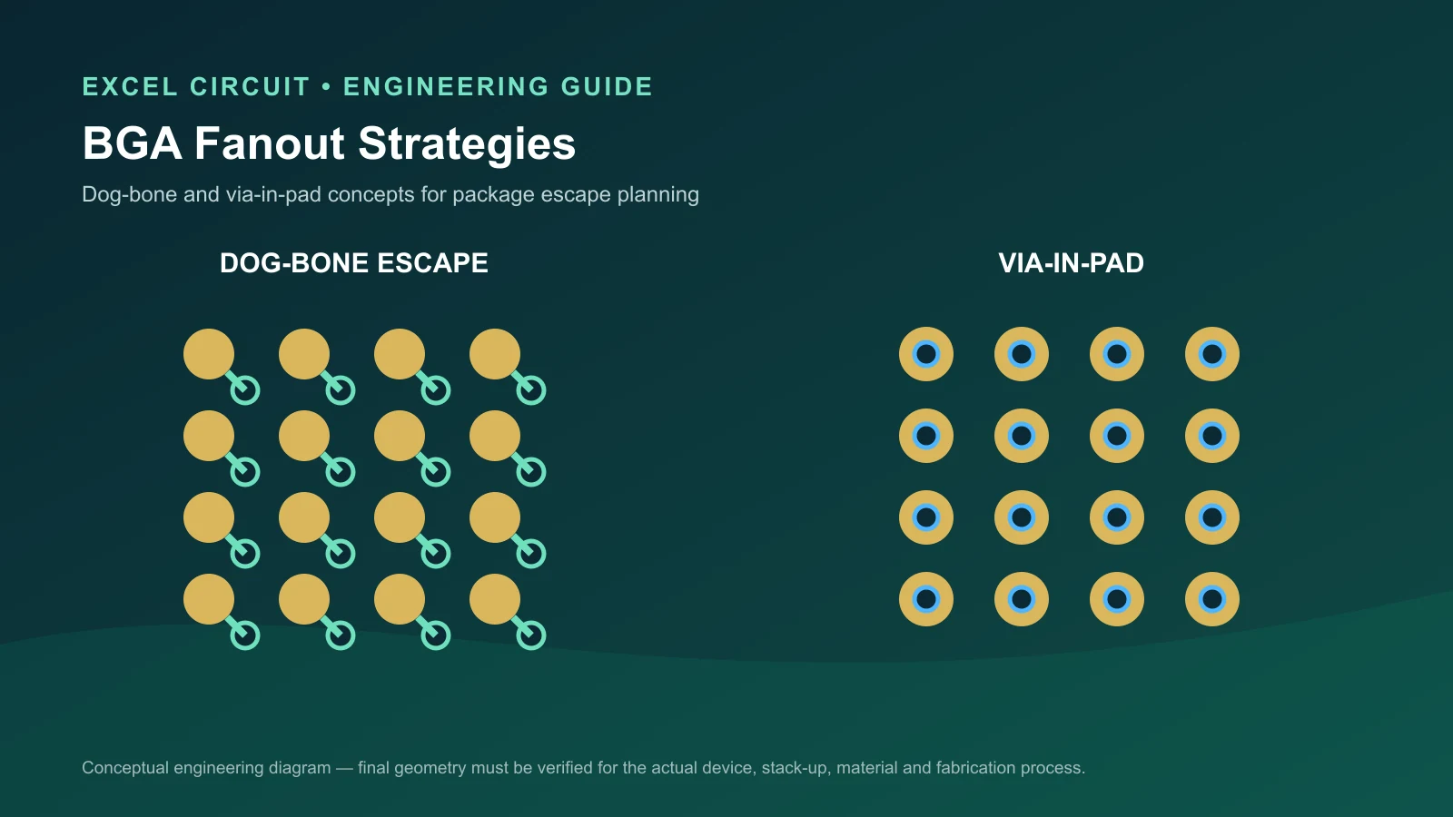
Dog-bone and via-in-pad fanout are options, not universal rankings. A design may use one method across the package or combine methods by region. The decision should reflect escape capacity, electrical behavior, fabrication complexity, assembly risk, and cost.
Dog-Bone Fanout
A dog-bone escape uses a short trace from the BGA land to a nearby via. It keeps the drilled structure outside the solderable pad and is often compatible with conventional through-via processing. Where the land pattern and supplier rules leave sufficient space, dog-bones provide a direct, inspectable approach without requiring a filled and plated-over pad.
The tradeoff is channel consumption. The offset via, its pad, and its antipad occupy routing area between rows and on internal planes. Deeper rows may need additional routing layers as outer channels fill. The short surface trace also creates a neck-down region whose geometry should be considered for controlled-impedance or high-current nets. Dog-bone orientation matters: a consistent radial pattern is easy to generate, but it may steer nets toward already congested board regions. Rotate or regionalize the escape direction according to the surrounding placement and downstream routing plan.
Via-in-Pad
Via-in-pad places a via within the component land, eliminating the offset dog-bone and releasing channel space. It can shorten transitions and enable direct access to build-up layers, which is useful in dense inner rows. It is not automatically required for every fine-pitch BGA, and it does not by itself guarantee that the remaining routing channels are sufficient.
The via structure and assembly surface must be documented with the fabricator. When the selected assembly and fabrication process requires a planar solderable land, the via may need filling, planarization, and copper plating over the opening. An open or poorly processed via in a BGA land can allow solder migration, reduce solder volume, or create surface nonplanarity. The exact fill and cap requirement is therefore conditional on via type, land design, supplier process, and assembly acceptance criteria. See the Via-in-Pad Technology Guide for process context, and coordinate the land pattern with BGA assembly and inspection.
A hybrid plan can be efficient: dog-bone the accessible outer rows, use via-in-pad only where row depth or signal priority justifies it, and protect power and reference connectivity throughout. This avoids both under-designing the dense core and applying premium processing where it adds little value.
Through-Via, Blind-Via and Microvia Strategies
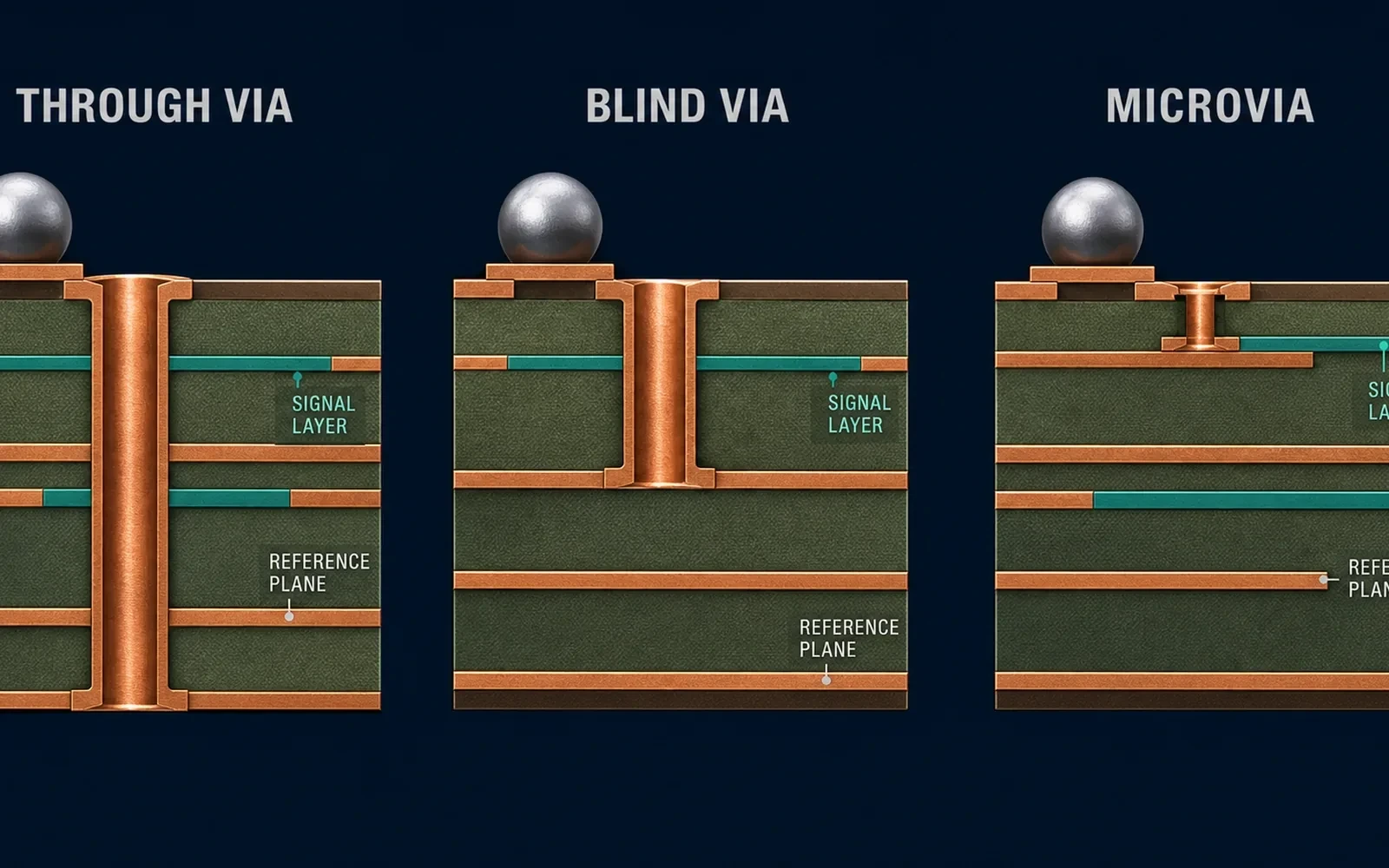
Via selection should follow the required layer connections and escape capacity. The terms through via, blind via, and microvia describe different aspects of construction; they should not be used as interchangeable labels.
Through-Via Strategy
A mechanically drilled through via connects the outer surfaces through the full board thickness. It is widely available and can support a robust, economical BGA breakout when pad pitch and channel geometry permit. Through vias may also connect power and ground across many layers efficiently.
Because the barrel crosses the entire stack, it creates antipads on every traversed plane and can block routing channels even on layers that do not use the connection. Unused barrel length may also matter for high-speed signals. The relevant question is not simply whether a through via fits near a pad, but whether its pad, drill tolerance, annular ring, antipad, and electrical transition fit the complete routing and plane plan.
Blind-Via Strategy
A blind via connects an outer layer to one or more internal layers without passing through the entire board. This frees deeper layers from the full through-hole barrel and may improve channel availability. Blind vias can be produced by different processes; the defining feature is the layer span, not a particular drill size. Their layer connections must align with the lamination sequence, and the design must state start and stop layers unambiguously.
Microvia Strategy
Microvias are considered when conventional through-via or dog-bone geometry cannot provide the required escape channels, or when the planned build-up stack needs short transitions between adjacent layers. They are not automatically required by a fine-pitch label. Their use depends on ball-map density, routing demand, via spans, reliability requirements, and a microvia construction qualified by the selected fabricator.
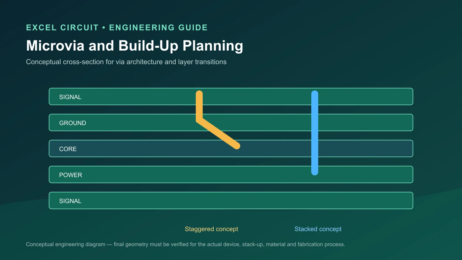
A microvia generally refers to a small via structure associated with HDI fabrication, commonly made with laser drilling in a thin dielectric. It may be blind, but “blind via” and “microvia” are not synonyms: blind describes connectivity, while microvia describes a type of structure and process. Microvias can move signals from a BGA land to an adjacent build-up layer and release channels on the core layers. Staggered, stacked, or skip configurations have different fabrication sequences and reliability considerations. Use only structures qualified by the selected supplier for the material system, copper construction, and reliability class.
Do not select stacking merely to make the layout visually compact. Check capture lands, dielectric thickness, copper fill, registration, thermal history, and the interaction with buried or through structures. The most suitable strategy is often mixed: through vias for accessible nets and power connections, limited blind or microvia transitions for dense rows, and layer changes positioned to preserve references.
How to Plan Escape Routing by BGA Density
Density is a system property rather than a label attached to pitch. Row depth, populated-ball percentage, net classes, usable channels, component placement, and fabrication rules determine how difficult the escape will be. A practical planning sequence is:
- Validate the source data. Confirm the package drawing, land pattern, pin-one orientation, ball names, no-connects, and permitted pin swaps before building fanout primitives.
- Map demand by region. Mark high-speed banks, clocks, analog nodes, power islands, grounds, low-speed controls, and unused balls. Count where nets must cross a package boundary rather than relying on total ball count.
- Assess surrounding placement. Identify nearby memory, connectors, power stages, heatsinks, keepouts, mounting features, enclosure boundaries, and adjacent components. These features determine which package edges are useful exits.
- Choose escape directions. Assign north, south, east, or west flow by functional destination. Do not fan every row radially if that pushes signals toward a blocked edge or forces unnecessary crossings.
- Estimate real channels. Apply the candidate trace, spacing, via pad, antipad, and registration rules to each routing layer. Subtract channels lost to plane clearances, reference stitching, power vias, and mechanical restrictions.
- Allocate layers and transitions. Give priority interfaces suitable routing layers and continuous references. Decide where dog-bone, through-via, blind-via, microvia, or via-in-pad structures are justified by the remaining capacity.
- Route representative worst cases. Test the deepest rows and the most constrained interface before repeating the pattern. Include differential pairs, power access, and escape paths toward actual destinations.
- Review and iterate. Run design checks, inspect planes and return paths, and review the proposed stackup with fabrication and assembly. Adjust placement, pin assignment, direction, or via architecture before broad routing makes change expensive.
Low-density regions can often use surface exits and conventional dog-bones. Medium-density regions may require deliberate layer allocation and mixed fanout. High-density cores may justify via-in-pad or build-up layers. These categories are descriptive, not fixed pitch bands. The proof is a routed, rule-correct channel model built with the intended manufacturing constraints.
BGA Fanout for High-Speed Interfaces
High-speed BGA fanout must preserve return-path continuity as signals leave the pad field and change layers; it is not only a routing-density problem. Via transitions and plane changes can interrupt the reference path even when trace geometry is correct. Layer transitions should therefore be planned with their reference planes, using nearby ground vias or an appropriate stitching strategy where the return path must move between references.
DDR, PCIe, processor, and FPGA interfaces make the BGA escape part of the interconnect rather than a neutral lead-in. Fanout geometry can introduce impedance changes, asymmetry, coupling, reference discontinuities, and via resonances before the main route begins. Broader constraint development belongs within high-speed PCB design; the BGA task is to carry those established requirements through the package breakout.
Keep differential members topologically similar through lands, neck-down regions, vias, antipads, and layer transitions. Exact visual symmetry is not always possible, but avoid giving one member an additional transition or a materially different reference environment without analysis. Treat clocks and strobes as priority nets and reserve their escape channels before low-speed signals consume the direct paths.
Controlled impedance may change through the narrow escape geometry. Use the shortest practical neck-down that meets fabrication rules and verify whether the discontinuity needs field-solver or channel-model review. When signals change layers, identify the reference plane on each layer and provide a nearby return-path connection where the reference changes. A signal via placed beside a void, split, or oversized merged antipad cannot rely on an abstract plane name to provide continuity.
Via transitions should be reviewed in the context of data rate, channel length, stackup, and unused barrel. That review may support a through via, a blind transition, backdrilling elsewhere in the channel, or a microvia approach, but the interface name alone does not mandate one. Preserve pair-to-pair spacing, avoid unnecessary parallelism inside the field, and check coupling created by dense via arrays. Package models, connector models, and memory topology may also influence pin escape order.
Finally, coordinate timing and length rules with the boundary of the fanout. Define whether delay or tuning measurements include the pad-to-via segment and which layer transitions belong to the matched group. This prevents the main routing area from compensating for an escape mismatch that was never included in the constraint model.
Power and Ground Escape Planning
Power and ground balls are not leftover connections to route after signals. They form the current path between the package, decoupling network, planes, and voltage-regulation system. Classify rails by function and transient demand, then reserve via access and plane connectivity before dense signal routing closes the available space.
Central power and ground regions may benefit from direct vias or via-in-pad connections, but the structure must be chosen with current distribution, assembly, and fabrication in mind. Use enough parallel connections to avoid concentrating current through narrow surface necks or isolated plane islands. At the same time, check that dense antipads do not perforate the plane so severely that the intended low-inductance path becomes a collection of bottlenecks.
Place decoupling components where their power and ground connections can reach the relevant BGA regions with short, coherent loops. Nearby memory, heatsinks, connectors, keepouts, mounting hardware, and components on the opposite side may restrict those locations. The placement study should include component body clearance, assembly access, and whether via fields interfere with capacitor lands.
Ground connections also support high-speed return paths. When signal escapes transition between reference planes, provide an appropriate nearby return connection based on the actual plane pair. Review split planes, voids, and antipad clusters visually rather than assuming connectivity from the netlist. For high-current or noise-sensitive rails, a PDN analysis can reveal plane spreading, via inductance, resonance, and decoupling issues that ordinary connectivity and clearance checks cannot.
BGA Fanout and PCB Stackup
PCB stackup determines which layers can accept BGA escapes, what reference plane each route uses, which via spans are buildable, and how antipads affect routing and plane continuity. Fanout and stackup should be planned together rather than sequentially. Adding layers without assigning usable channels, references, and transitions may increase cost without resolving the actual congestion.
Begin with signal-reference needs, power distribution, material constraints, board thickness, copper construction, and the routing demand beneath the BGA. Then assign escape layers and via spans that the fabricator can build.
For each routing layer, record its preferred escape direction, reference plane, applicable trace geometry, and the BGA rows it is expected to serve. Confirm that plane antipads leave both routing room and adequate copper continuity. If build-up layers are proposed, document dielectric construction, capture relationships, lamination sequence, and whether microvias are staggered or stacked. If conventional through vias are used, account for their barrels and antipads across the complete board.
Stackup decisions also affect high-speed transition behavior and power integrity. A layer that appears geometrically convenient may reference a power island, cross a plane boundary, or require an avoidable reference change. Conversely, a well-placed ground plane can support escape routing and shielding while simplifying return-path stitching.
Review the stackup with the selected fabricator before layout is locked. The review should cover material availability, copper balance, drill processes, registration, via fill, planarization, impedance requirements, and inspection. Keep the released stackup, via table, and fabrication notes consistent; discrepancies between these documents can turn an otherwise correct fanout into an ambiguous build.
Common BGA Fanout Routing Mistakes
- Selecting a via strategy before the stackup. The proposed spans may not match a buildable lamination sequence or suitable references.
- Estimating difficulty from pin count alone. Row depth, populated regions, pin distribution, destination, and available exits matter more than a single total.
- Counting nominal channels. Via antipads, plane clearances, differential spacing, registration allowances, and power vias reduce real capacity.
- Routing signals before power and ground. This can leave central rails connected by long necks and block reachable decoupling paths.
- Ignoring reference continuity. A clearance-correct trace may still cross a plane void or transition without a suitable return connection.
- Adding unnecessary layer transitions. Extra vias consume channels and can complicate high-speed behavior, inspection, and documentation.
- Using generic fabrication limits. Advertised minimums may not apply to the selected material, copper, panel, reliability target, or production volume.
- Leaving via-in-pad processing ambiguous. Fill, planarization, plating, and acceptance requirements must be stated when the chosen process requires them.
- Specifying HDI construction without supplier coordination. Stacked, staggered, or skip structures must match a qualified build and reliability basis.
- Freezing placement without mechanical context. Memory, connectors, heatsinks, keepouts, mounting holes, enclosure limits, and adjacent components can block the intended escape direction.
How to Check BGA Escape Routing Before Release
A clean design-rule check is necessary, but it is not complete proof of fabricability. DRC verifies the encoded rules; it may not know the supplier’s process conditions, lamination restrictions, via-fill requirements, reliability limits, assembly risks, or whether the intended return path remains electrically sound. Complete these release checks:
- Reconcile the schematic, verified package drawing, land pattern, pin map, and pin-one orientation.
- Review every BGA region for intended escape direction, layer assignment, crossings, and blocked exits.
- Check trace, space, drill, pad, annular ring, antipad, solder-mask, and registration rules against the selected supplier’s approved values.
- Inspect signal references, plane voids, return transitions, differential symmetry, and high-speed via structures.
- Review power and ground connectivity, neck-downs, plane fragmentation, decoupling access, and current paths.
- Verify the stackup, via table, start/stop layers, fill and cap notes, sequential lamination, and fabrication drawing agree.
- Check component placement, keepouts, heatsinks, connectors, mounting features, enclosure constraints, and assembly or inspection access.
- Run fabrication and assembly review using the PCB design for manufacturability guidelines and obtain project-specific feedback through a DFM/DFA Review service before production release.
When HDI Is Useful for BGA Fanout
HDI is useful when conventional fanout cannot provide enough usable escape channels, when full through-via antipads block required inner-layer routing, or when short controlled transitions materially help the electrical architecture. It may also support compact placement where the dense BGA must connect to nearby memory or other fine-pitch packages without expanding the board.
The decision should be demonstrated with routing demand and a buildable stackup. Start by testing conventional dog-bone and through-via options using the selected fabricator’s rules. If the deepest rows, priority interfaces, power access, or return paths remain constrained, evaluate whether limited build-up layers or via-in-pad microvias solve those specific regions. A hybrid architecture is often more economical and easier to qualify than applying the most advanced structure everywhere.
HDI adds coordination requirements. Laser-drilled structures, thin dielectrics, capture pads, copper fill, stacked or staggered transitions, and sequential lamination must be defined as a coherent construction. Yield, inspection, material availability, thermal cycling, and the supplier’s qualified reliability data belong in the decision. A visually routable layout is not enough if its via sequence cannot be manufactured repeatably.
Use HDI PCB design when the project benefits from integrated package breakout, build-up planning, signal and power integrity, and supplier alignment. Do not use the “fine-pitch” label alone as justification. The engineering objective is the least complex architecture that meets routing, electrical, mechanical, assembly, and reliability requirements.
Engineering Checklist
Before BGA fanout planning begins, gather the released package drawing and ball map, verified land pattern, placement and mechanical constraints, interface and pin-group priorities, power and ground requirements, preliminary stackup, and the intended fabricator’s design rules. Assembly requirements and any via-in-pad or HDI assumptions should also be available so the escape plan is based on one consistent project release.
- Package drawing, land pattern, pin map, and orientation verified.
- Signal, power, ground, high-speed, and priority groups classified.
- Surrounding placement and escape directions reviewed.
- Escape-channel estimate completed with real fabrication rules.
- Fanout method justified for each BGA region.
- Stackup, routing layers, references, and build-up sequence approved.
- Differential transitions and reference-plane changes reviewed.
- Antipads checked for routing loss and plane fragmentation.
- Power paths, ground returns, and decoupling access reserved.
- Via-in-pad fill, planarization, and plating requirements documented when applicable.
- Blind-via spans and microvia stacking or staggering rules confirmed.
- Mechanical, assembly land-pattern, and inspection constraints reviewed.
- Project-specific fabrication and assembly DFM completed before production release.
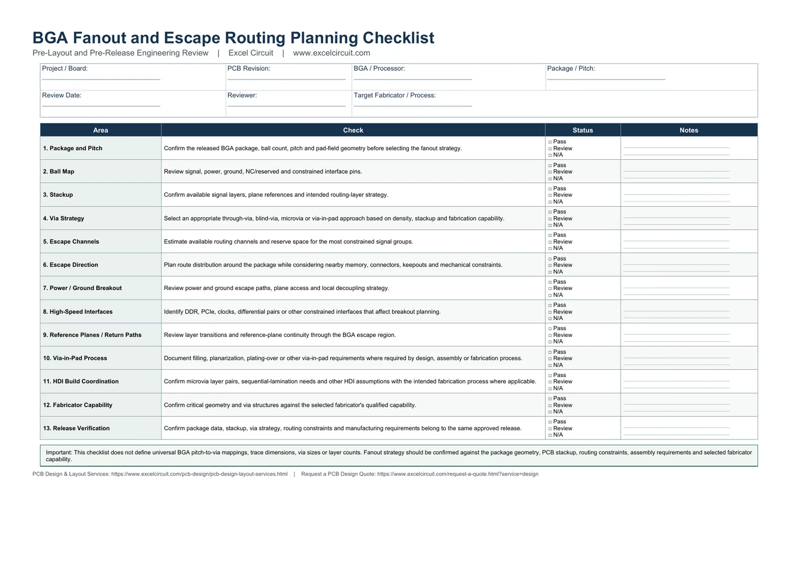
Download the BGA Fanout Planning Checklist
Use this one-page printable checklist to review the BGA package, ball map, stackup, via strategy, high-speed constraints, power/ground breakout and fabrication assumptions before detailed routing or manufacturing release.
FAQ
What is BGA fanout in PCB design?
BGA fanout is the process of moving signal, power, and ground connections from the BGA ball field into routable PCB channels. It may use surface traces with dog-bone geometry, via-in-pad, through vias, blind vias, microvias, or a combination selected for different package regions. The appropriate fanout strategy depends on package pitch, ball map, stackup, routing density, electrical constraints, and the selected fabricator’s qualified capability.
What is the difference between BGA fanout and escape routing?
The terms are closely related and are sometimes used interchangeably. Fanout generally emphasizes bringing connections from BGA lands into vias or other breakout geometry. Escape routing emphasizes carrying those signals beyond the congested ball field into an area where normal board routing can continue. In practice, both activities should be planned together because fanout geometry determines the channels, layer transitions, references, and directions available to the escape routes.
When should I use dog-bone fanout instead of via-in-pad?
Dog-bone fanout may be practical when package geometry and routing space provide sufficient escape channels around offset vias. Via-in-pad may become useful when pitch, row depth, channel availability, or the selected HDI architecture makes external dog-bone breakout too constrained. Neither method is universally better. The final choice also depends on stackup, via process, fabricator capability, assembly requirements, electrical performance, and cost.
Does a fine-pitch BGA always require HDI?
No. Fine-pitch packages often make HDI techniques useful, but they do not create a universal HDI requirement. The actual need depends on the ball map, package pitch, routing density, available layers, via strategy, board geometry, electrical constraints, and fabrication capability. Some designs can use conventional dog-bone or through-via fanout, while denser regions may benefit from a hybrid or build-up approach.
How many PCB layers are needed for BGA fanout?
There is no universal layer count. The required routing strategy depends on package density, signal groups, usable escape channels, power and ground distribution, high-speed reference needs, via spans, and the complete stackup. Two BGAs with similar pin counts can require different routing-layer plans because their ball maps, destinations, board geometry, and fabrication constraints are different.
How should BGA escape routing be checked before fabrication?
Verify the package and ball map, land pattern, stackup, via types and layer pairs, power and ground breakout, high-speed return paths, and the selected fabricator’s capabilities. Confirm that via-in-pad processing is documented where applicable and that the layout, via table, stackup, and fabrication notes agree. Design-rule checks should be followed by project-specific fabrication and assembly DFM review before release.
Working on a Fine-Pitch BGA or FPGA Board?
Need a project-specific BGA layout review? If your design involves a dense BGA, FPGA, high-speed interfaces, or HDI fanout constraints, send the available schematic, package information, board requirements, and design constraints for an engineering review and layout quotation. Request a PCB Design Quote.