Contents
A PCB stackup defines the vertical arrangement of copper signal layers, reference and power planes, copper foil, cores, prepregs and other dielectric materials in a multilayer board. It is an electrical and manufacturing architecture, not just a layer list: the construction influences controlled impedance, return-current paths, routing density, EMI, power distribution, via options, board thickness and fabricability. A usable stackup connects those requirements before detailed layout begins.
Why Stackup Planning Comes Before Detailed Routing
PCB stackup should be planned before routing because trace rules, impedance geometry, reference paths, routing-layer capacity, BGA escape, power distribution and via spans all depend on the physical construction. Routing and stackup planning are interdependent: freezing routes against an assumed build can force width changes, reference discontinuities, extra transitions or a layer redesign when the selected fabricator supplies the real dielectric and copper construction.
Start with the board outline, thickness and connector constraints; critical interfaces and impedance requirements; package and BGA density; power rails and current paths; thermal needs; and the qualified fabrication processes under consideration. Assign electrical purposes to layers before selecting a final count. The related PCB design and layout services page describes project support, while this guide focuses on the engineering decisions themselves.
Core, Prepreg, Copper and Layer Functions
Core and Prepreg
A core is a cured dielectric laminate with copper on one or both sides before processing. Prepreg is resin-impregnated reinforcement used to bond layers during lamination; its pressed thickness and dielectric behavior depend on the selected construction and process. Both influence finished separation between conductors, impedance, overall thickness, material availability and lamination feasibility.
Copper Foil, Signal Layers and Planes
Copper foil forms outer or inner conductive layers before etching and plating. Signal layers carry routed interconnects. Ground and power planes distribute reference or rail connections, but “reference plane” is the broader electrical term: a signal may reference ground or another appropriate low-impedance structure depending on the interface and return architecture. A power plane is not automatically a suitable reference across every split or frequency.
Pair High-Speed Signal Layers With Intentional References
High-speed signal layers generally benefit from an adjacent continuous reference plane because the nearby reference supports a compact return-current path, controlled field geometry, smaller loop area and more predictable impedance. Poor pairing can enlarge return loops, expose routes to plane gaps, complicate impedance control and increase coupling or EMI risk. The required arrangement depends on interface behavior and construction, not one universal signal-to-plane spacing.
Each critical routing layer should have an intentional reference over the complete route. Adjacent signal layers are not automatically problematic, and orthogonal routing is not a universal cure: coupling depends on separation, reference-plane shielding, parallel exposure, edge rate and field geometry. A solid reference plane between routing layers can provide stronger isolation than relying on direction alone.
Stackup Defines the Return-Current Structure
A high-frequency signal current completes a loop, and its return tends to follow a low-impedance path near the signal’s reference structure. The stackup determines which reference is adjacent and whether transitions can be supported. Plane splits, voids, connector transitions and changes between reference layers can interrupt that path even when the trace geometry itself appears correct.
When a signal changes layers, review how its return transfers between the old and new references. A nearby stitching or grounding connection may be appropriate when the reference structures and net relationships support it, but every transition does not require an identical pattern. A controlled-impedance trace can still perform poorly if its return loop is disrupted; a ground plane does not simply “eliminate noise.”
How Stackup Determines Controlled Impedance
Stackup determines controlled impedance through the combination of trace width, finished copper thickness, dielectric thickness and dielectric constant, reference-plane location, trace type and fabrication process. Outer-layer microstrip geometry may also be influenced by solder mask; inner stripline geometry depends on the surrounding dielectric and reference arrangement. Stackup and impedance must therefore be solved together, then confirmed using the selected fabricator’s production construction.
A width copied from another layer or project is not a reliable rule because its copper, dielectric and reference geometry may differ. Record target nets, routing layers, reference layers and impedance requirements, then let the agreed production stackup drive CAD rules. When interface risk warrants deeper review, SI/PI analysis and high-speed PCB design support can test the implemented structure rather than an unrelated nominal model. For a concrete application, the 50-ohm PCB trace design guide explains how production geometry is calculated and verified.
Microstrip and Stripline Are Trade-Offs
Microstrip routes are on an outer layer with a reference plane beneath and greater exposure to external fields. Stripline routes are inside the board with reference planes surrounding the signal according to the construction, generally providing stronger field containment. Neither is universally superior: accessibility, conductor and dielectric loss, routing density, EMI, fabrication geometry and the need for via transitions all affect the choice.
Signal Integrity Begins With the Stackup
PCB stackup affects signal integrity by establishing transmission-line geometry, dielectric and conductor loss, reference continuity, coupling environment and the via transitions available between layers. These choices influence reflection, crosstalk, insertion loss, timing and EMI before detailed routing is complete. Simulation can evaluate a proposed architecture, but it cannot recover performance if the released physical build no longer matches the modeled stackup and routing assumptions.
Distance to the reference, trace separation, parallel coupling length, layer arrangement and edge rate all influence crosstalk. Avoid fixed spacing multipliers as guarantees. Use interface-specific rules and validate sensitive structures where appropriate. Adjacent routing layers may use different directions to reduce long parallel exposure, but reference-plane isolation and actual geometry matter more than a blanket orthogonal-routing statement.
Power Integrity and the Role of Power Planes
PCB stackup affects power integrity through power/ground layer placement, plane and via impedance, rail distribution, current-loop geometry, decoupling access and the coupling between conductive structures. Closely coupled plane pairs can contribute distributed capacitance and low-inductance paths, but they do not replace discrete decoupling or package-level connections. PDN design must consider source, planes or pours, vias, capacitors, package and return as one network.
Dedicated power planes may help broad current distribution, reduce DC resistance and simplify a major rail. They are not mandatory for every multilayer board. Multiple rails can fragment a plane, reduce routing flexibility or increase layer count; pours and local structures may be more suitable in some designs. Any split beneath a signal route must be reviewed for return-path consequences.
BGA, FPGA and DDR Stackup Planning
Stackup influences BGA escape by determining how many usable routing layers exist, which references support them, what via spans are possible, how power and ground balls connect, and where high-speed groups can leave the package. Package pitch alone does not dictate a layer count or via type. Escape direction, ball map, destination, channel geometry, impedance and the fabricator’s qualified processes must be evaluated together.
The HDI and fine-pitch BGA engineering example shows how package, via and layer decisions interact without creating a universal prescription. For FPGA and DDR designs, reserve appropriate references and routing capacity for memory and high-speed groups before general routing consumes the channels.
HDI and Via Architecture Must Be Part of the Stackup
Through vias, blind and buried vias, microvias, via-in-pad and back-drilled structures use different layer spans and manufacturing sequences. HDI may add buildup layers and sequential lamination, but architectures such as 1+N+1 or 2+N+2 are examples, not mandatory formulas. Select the least complex structure that meets escape, transition, density and reliability requirements.
Plan capture pads, antipads, unused stubs, fill/cap needs and reference transitions with the layer order. The HDI PCB Design service covers project-specific support, while the HDI PCB Design Complete Guide explains buildup, microvia and via-in-pad options in depth.
When Low-Loss or RF Materials Are Needed
Low-loss or RF laminate should be considered when the operating frequency, insertion-loss budget, phase consistency, impedance geometry, thermal environment or reliability requirements cannot be met confidently with the available general-purpose material system. Not every RF board requires a branded microwave laminate. Compare frequency-dependent Dk and Df, conductor loss, material consistency, fabrication compatibility, availability and cost for the actual route lengths and performance margin. Apply the material choice within the full RF PCB design, including launches, references, grounding, and tolerances.
FR-4 describes a broad family rather than one fixed dielectric constant. High-Tg and low-loss grades can differ in Dk, Df, thermal behavior, z-axis expansion and process availability. RF stackups also require reference continuity and grounding strategy; laminate selection alone does not create RF performance. Material substitutions should preserve the properties used by the impedance and loss analysis.
Copper Thickness, Board Thickness and Layer Count
Copper Thickness Is Not a One-Direction Upgrade
Thicker copper can support current and reduce DC resistance for a given geometry, but it also changes impedance, etching behavior, spacing capability, lamination and compensation. Tight geometry can become harder to reproduce as copper increases. Current capacity must be evaluated using copper geometry, allowable temperature rise, airflow, board construction and applicable standards—not a single width chart. For routing-specific limits, review high-current copper and via design.
Total Board Thickness Is a Project Constraint
Total thickness can be driven by mechanics, connectors, impedance, layer count, materials, stiffness, via aspect ratio and manufacturing capability. A 1.6 mm board is a common example in the industry, not a mandatory standard. Confirm finished thickness and tolerance against the enclosure, connector and selected construction.
How Many PCB Layers Are Needed?
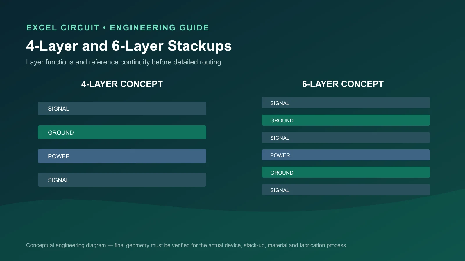
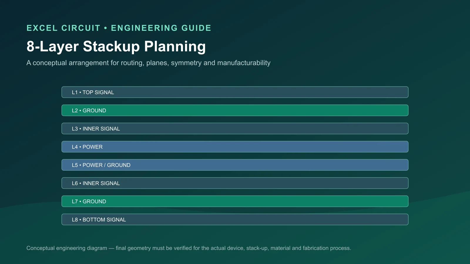
There is no universal PCB layer count; it should be justified by routing density, BGA escape, reference-plane needs, controlled-impedance signals, power rails, EMI risk, mechanics, via architecture, fabrication capability and cost. Four-, six- or eight-layer arrangements can be useful illustrative architectures, but none is automatically correct. Assign electrical functions and estimate routing channels before selecting the smallest practical construction that satisfies the project.
Coordinate the Final Stackup With the PCB Fabricator
Before releasing a stackup, confirm available cores and prepregs, pressed dielectric thicknesses, finished copper, laminate availability, total thickness, controlled-impedance capability, via spans, aspect ratios, sequential lamination and HDI processes with the selected fabricator. Update the PCB rules and fabrication drawing to the approved construction. Any substitution or thickness change should be reviewed because it can alter impedance, loss, stubs, coupling and reliability.
Excel Circuit supports fabricator coordination through qualified PCB manufacturing resources; it does not claim an in-house PCB fabrication plant. The engineering objective is to align stackup, impedance, BGA breakout, SI/PI and DFM with project requirements and a buildable production route. The existing PCB manufacturing support page describes that broader coordination.
Stackup DFM and Common Release Mistakes
Stackup DFM should check material availability, dielectric construction, copper balance, total thickness, impedance feasibility, via aspect ratio, drill structure and lamination sequence. A nominal CAD stackup is not production approval. Review unusual requirements before routing is frozen and use project-specific manufacturing feedback.
- Routing high-speed signals without an adjacent continuous reference.
- Crossing plane splits or changing references without reviewing the return path.
- Adding layers without assigning an electrical or routing purpose.
- Selecting layer count only from nominal fabrication price.
- Freezing trace geometry before confirming the production stackup.
- Ignoring BGA escape and via spans during layer planning.
- Treating power planes as automatic SI or decoupling solutions.
- Choosing specialty laminate without a loss, consistency or reliability reason.
- Releasing drawings and CAD rules that reference different revisions.
| Stackup decision | Electrical impact | Manufacturing impact |
|---|---|---|
| Signal-to-reference construction | Return path, impedance and field containment | Available core/prepreg thicknesses |
| Finished copper | Current path and impedance geometry | Etching, plating and spacing capability |
| Material system | Dk, Df, thermal and loss behavior | Availability, lamination and approved substitutions |
| Via structure | Routing access, stubs and reference transitions | Drilling, fill/cap and lamination complexity |
| Layer count and functions | Routing capacity, references and rail distribution | Thickness, registration, process steps and cost |
| Construction balance | May constrain layer arrangement | Bow, twist and lamination behavior |
PCB Stackup Review Checklist
- Board outline, finished thickness, connector and mechanical requirements confirmed.
- Layer count justified by electrical and routing functions.
- Every critical signal layer has an intentional continuous reference.
- Return paths and reference changes reviewed.
- Impedance targets, layers, geometry and references defined.
- Power rails, plane splits, decoupling access and current paths reviewed.
- BGA escape, routing channels and via spans checked.
- Materials, copper weights and acceptable substitutions documented.
- Core/prepreg construction and total thickness confirmed.
- HDI or sequential-lamination sequence documented where applicable.
- Copper balance, via aspect ratio and impedance feasibility reviewed.
- Selected fabricator approved the stackup and PCB rules match its revision.
FAQ
How many PCB layers are required?
It depends on routing density, reference-plane needs, power distribution, package escape, impedance structures, mechanical limits, and fabrication technology. Estimate functions and channels before choosing the count.
What dielectric thickness should be used?
There is no universal thickness. It must be selected with impedance, field containment, trace geometry, material availability, copper thickness, and fabrication capability.
Should every signal layer have an adjacent ground plane?
Critical high-speed layers should have a continuous defined reference. Ground is often preferred, but the complete return-path and power-distribution architecture determines the correct arrangement.
Can the manufacturer change the stack-up?
Changes should be reviewed and approved because they can alter impedance, loss, via stubs, coupling, and reliability. The design rules and fabrication drawing must remain synchronized with the production stack-up.
Request a PCB Stackup Engineering Review
If you are defining a multilayer PCB stackup, share the schematic, board outline, BGA/package information, critical interfaces, impedance requirements and fabrication constraints for engineering review.