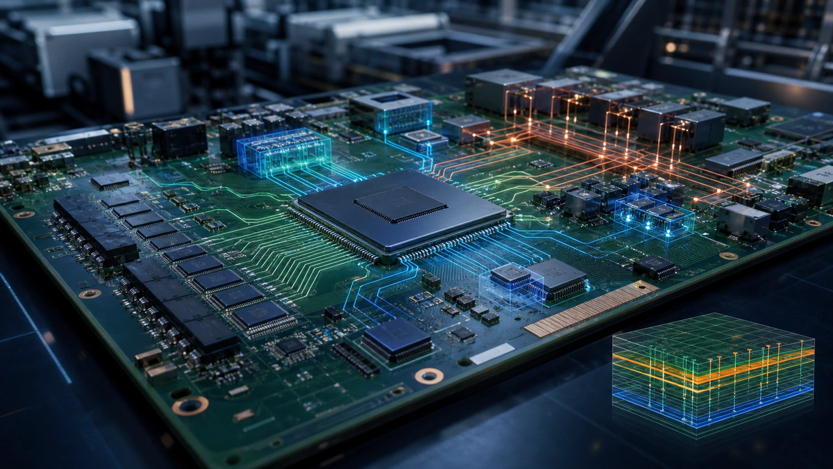
Featured Article
Embedded & FPGA PCB Design: From Architecture to Reliable Bring-Up
A practical engineering guide covering architecture, power sequencing, DDR routing, SI/PI verification, DFM, and reliable board bring-up.
Read Featured Article
A practical engineering guide covering architecture, power sequencing, DDR routing, SI/PI verification, DFM, and reliable board bring-up.
Read Featured Article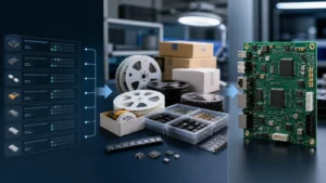
A production-ready PCB assembly BOM should identify each component by reference designator, quantity per board, manufacturer, manufacturer part number, value or description, and package or footprint. It should
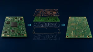
To export Gerber files from Altium Designer for PCB manufacturing, open the approved PCB document and use File » Fabrication Outputs » Gerber Files. Configure Gerber or Gerber
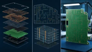
Before sending a PCB design for manufacturing, verify that the fabrication package contains the correct copper, solder mask, silkscreen, board outline and NC drill data. Confirm that the
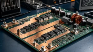
Engineering guidelines for high-current PCB layout covering copper paths, via arrays, switching loops, heat spreading, safety spacing and manufacturing.
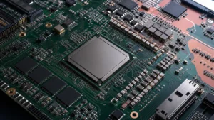
Engineering guidelines for FPGA power integrity, PDN design, decoupling placement, BGA power delivery, plane transitions, sequencing and PI validation.
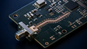
Engineering guide to 50-ohm RF PCB traces covering microstrip, stripline, coplanar waveguide, stack-up variables, connector transitions and fabrication tolerance.
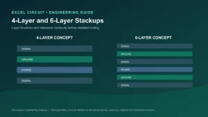
An engineering guide to PCB stackup design covering layer functions, reference planes, power distribution, materials, controlled impedance, via architecture, construction balance and manufacturing DFM.
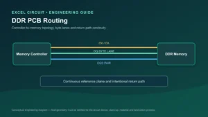
Engineering-focused DDR PCB routing guidelines covering topology, timing budgets, byte-lane constraints, length matching, impedance, return paths, SI/PI and manufacturing review.
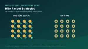
An engineering guide to BGA fanout covering escape-channel planning, dog-bone routing, via-in-pad, microvias, stack-up coordination, return paths, power delivery and manufacturing DFM.
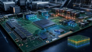
A practical engineering guide to Embedded & FPGA PCB design, from architecture and power sequencing to DDR routing, SI/PI verification, DFM, and board bring-up.