
Featured Article
Embedded & FPGA PCB Design: From Architecture to Reliable Bring-Up
A practical engineering guide covering architecture, power sequencing, DDR routing, SI/PI verification, DFM, and reliable board bring-up.
Read Featured Article
A practical engineering guide covering architecture, power sequencing, DDR routing, SI/PI verification, DFM, and reliable board bring-up.
Read Featured Article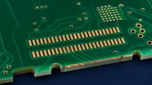
Review PCB solder mask openings, expansion, dams and pad or via treatment. Coordinate package recommendations, registration and exposed copper with fabrication and assembly requirements.
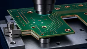
Understand variation in PCB traces, holes, outlines and thickness. Identify critical dimensions and document tolerance requirements that match electrical function, mechanical fit and the proposed fabrication process.
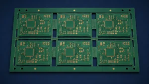
Choose a PCB array and breakaway method around board geometry, assembly handling and finished edge requirements. Compare V-scoring, routed tabs, tooling rails and depanelization risks.
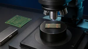
Define the required PCB and PCBA quality level without confusing fabrication, soldering and assembly acceptance. Covers selection, documentation and quotation requirements.
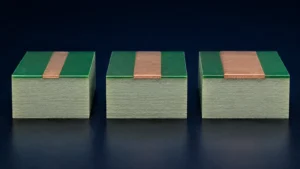
Choose PCB copper by layer with a clear view of conductor geometry, finished thickness, via transitions and manufacturing constraints. Includes a practical review checklist.
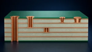
A manufacturing-focused comparison of through, blind, buried and microvia structures, with via-in-pad considerations and the inputs needed to review a multilayer interconnect.
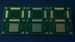
Select a PCB surface finish around soldering, pad flatness, storage, RF, contacts and wire bonding rather than assuming one finish is best for every board.
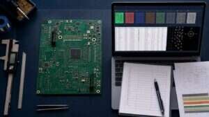
A complete PCB manufacturing file checklist covering Gerber or ODB++, NC drill data, fabrication drawings, BOM, pick-and-place files and test requirements.
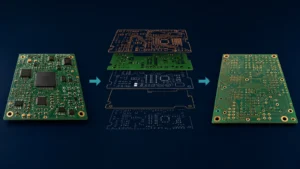
To export Gerber files from Altium Designer for PCB manufacturing, open the approved PCB document and use File » Fabrication Outputs » Gerber Files. Configure Gerber or Gerber
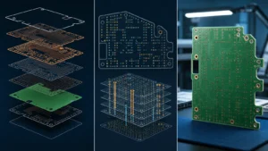
Before sending a PCB design for manufacturing, verify that the fabrication package contains the correct copper, solder mask, silkscreen, board outline and NC drill data. Confirm that the